Two-dimensional silicon controlled rectifier

a rectifier and silicon technology, applied in the direction of diodes, semiconductor devices, electrical apparatus, etc., can solve the problems of design compromise, design may not be able to achieve the width of the scr that is necessary for the desired current handling capability, etc., to achieve the effect of increasing the physical scr area, increasing the anode to cathode contact length, and maximizing the contact length

Inactive Publication Date: 2006-01-19
SOFICS BVBA
View PDF5 Cites 23 Cited by
  • Summary
  • Abstract
  • Description
  • Claims
  • Application Information

AI Technical Summary

Benefits of technology

[0011] The present invention is a two-dimensional silicon controlled rectifier (2DSCR) having the anode and cathode forming a checkerboard pattern. Such a pattern maximizes the anode to cat...

Problems solved by technology

If the region of the circuit in which the SCR is formed has limited space for the SCR width, the designer may not be able to ...

Method used


Image

  • Two-dimensional silicon controlled rectifier
  • Two-dimensional silicon controlled rectifier
  • Two-dimensional silicon controlled rectifier

Examples


Embodiment Construction

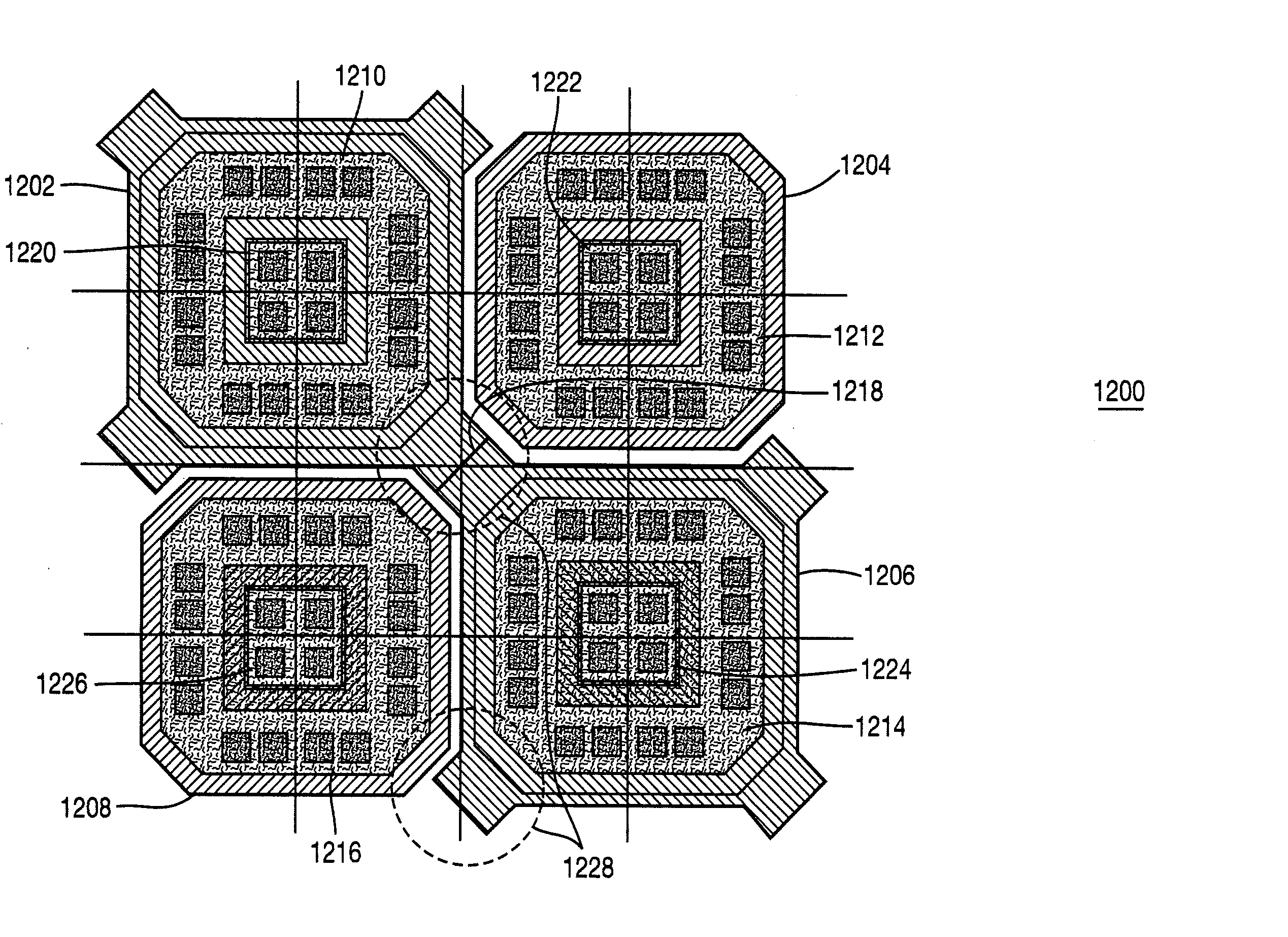
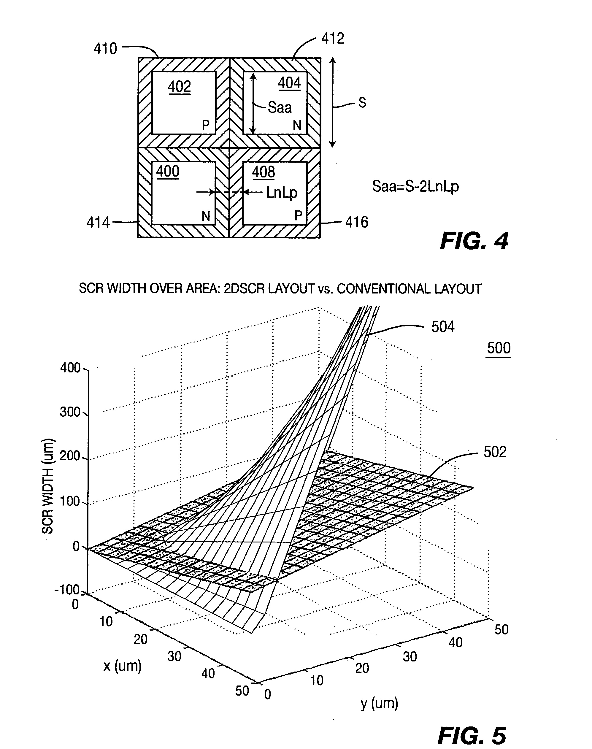
[0025] The present invention is a two-dimensional silicon controlled rectifier (2DSCR) having an anode and cathode arranged in a checkerboard pattern. Such a pattern increases the effective width of the SCR and enables the current handling capability to be controlled by the area of the SCR, i.e., in two-dimensions.

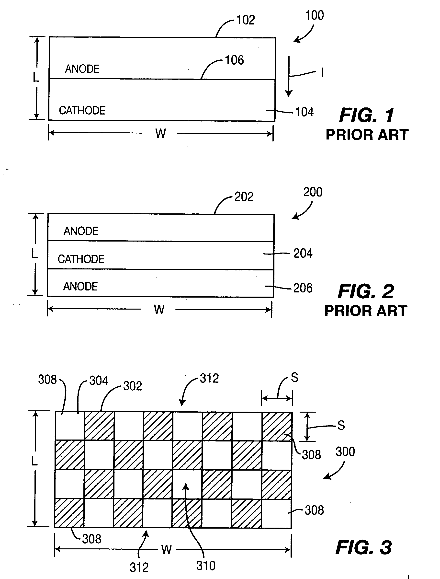
[0026]FIG. 3 depicts a simplified top plan view of a 2DSCR 300 comprising a plurality of anodes 302 and cathodes 304 arranged in a checkerboard pattern. Each anode 302 and cathode 304 is substantially square where the active edges of the anode and cathode regions are substantially equal in length. Such a structure provides functional uniformity. However, in some designs, an asymmetric function may be desirable such that rectangular or other shaped anode and cathode regions may be used.

[0027] The anodes and cathodes are positioned alternately next to each other in rows and columns to form the checkerboard pattern. In a layer or layers above the pattern (but not shown in F...


PUM


Abstract

A two-dimensional silicon controlled rectifier (2DSCR) having the anode and cathode forming a checkerboard pattern. Such a pattern maximizes the anode to cathode contact length (the active area) within a given SCR area, i.e., effectively increasing the SCR width. Increasing the physical SCR area, increases the current handling capabilities of the SCR.

Description

CROSS-REFERENCE TO RELATED APPLICATIONS [0001] This application claims benefit of U.S. provisional patent application Ser. No. 60 / 585,934, filed Jul. 7, 2004, which is herein incorporated by reference.BACKGROUND OF THE INVENTION [0002] 1. Field of the Invention [0003] Embodiments of the present invention generally relate to a silicon controlled rectifier (SCR) layout within an integrated circuit (IC) and, more particularly, to an SCR layout that maximizes the width / area ratio of an SCR layout. [0004] 2. Description of the Related Art [0005] Silicon-controlled rectifiers (SCRs) find widespread use in many applications where a switched resistive path is desired. For example, SCRs find particular use in electrostatic discharge (ESD) circuits or devices that are placed between an output or input pad of an IC and ground. The ESD circuits provide a high resistance path through an SCR when the circuit being protected is operating normally, and provides a low resistance path from the pad to...

Claims


Application Information

Patent Timeline
IPC IPC(8): H01L29/32
CPCH01L27/0259H01L27/0262H01L29/87H01L29/74H01L29/7436H01L29/0692
Inventor MOHN, RUSSELLTRINH, CONG-SONJOZWIAK, PHILLIP CZESLAWARMER, JOHNMERGENS, MARKUS PAUL JOSEF
Owner SOFICS BVBA
Why Eureka
Try Eureka