2-Terminal semiconductor device using abrupt metal-insulator transition semiconductor material

a transition semiconductor and metal-insulator technology, applied in the field of semiconductor devices, can solve the problems of switching devices, memory devices may break, devices cannot be used for other applications, etc., and achieve the effect of low cost and easy formation

Inactive Publication Date: 2006-01-19
ELECTRONICS & TELECOMM RES INST
View PDF16 Cites 60 Cited by
  • Summary
  • Abstract
  • Description
  • Claims
  • Application Information

AI Technical Summary

Benefits of technology

[0008] The present invention provides a 2-terminal semiconductor device that uses an abrupt MIT semiconductor material that can be formed readily with a low cost without generating a structural phase transition.

Problems solved by technology

However, the device cannot be used for other applications, such as a switching device, because a rapid switching speed cannot be implemented due to the location change of atoms according to the structural phase transition.
If a rapid switching speed is forced, the memory device may break due to a hysteresis phenomenon.
A drawback of the phase change memory device is its limited applications.
However, if the dielectric constant is too high, the lifetime of the transistor is reduced since the fatigue characteristic of the dielectric may go badly at a high switching speed.
There is a process limit to make a thin insulator.
Also, when the gate voltage is high, there is a drawback of high power consumption.
However, the availability of the abrupt MIT semiconductor materials is limited and the cost of forming an abrupt MIT semiconductor material layer is high.

Method used


Image

  • 2-Terminal semiconductor device using abrupt metal-insulator transition semiconductor material
  • 2-Terminal semiconductor device using abrupt metal-insulator transition semiconductor material
  • 2-Terminal semiconductor device using abrupt metal-insulator transition semiconductor material

Examples


Embodiment Construction

[0068] The present invention will now be described more fully with reference to the accompanying drawings in which exemplary embodiments of the invention are shown. However, this invention may be embodied in many different forms and should not be construed as being limited to the embodiments set forth herein.

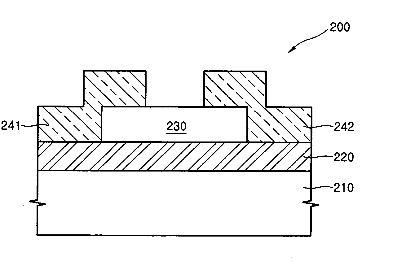
[0069]FIG. 1 is a cross-sectional view illustrating a 2-terminal semiconductor device 100 that uses an abrupt MIT semiconductor material according to an embodiment of the present invention.

[0070] Referring to FIG. 1, the 2-terminal semiconductor device 100 has a stacking structure in which a current flows in a vertical direction and includes sequentially stacked a buffer layer 120, a first electrode layer 141, an abrupt MIT semiconductor material layer 130, and a second electrode layer 142 on a substrate 110. In some cases, the substrate 110, the buffer layer 120, and the first electrode layer 141 can be formed of a single layer. In this case, the first electrode layer 141 act...


PUM


Abstract

Provided is a 2-terminal semiconductor device that uses an abrupt MIT semiconductor material layer. The 2-terminal semiconductor device includes a first electrode layer, an abrupt MIT semiconductor organic or inorganic material layer having an energy gap less than 2eV and holes in a hole level disposed on the first electrode layer, and a second electrode layer disposed on the abrupt MIT semiconductor organic or inorganic material layer. An abrupt MIT is generated in the abrupt MIT semiconductor material layer by a field applied between the first electrode layer and the second electrode layer.

Description

BACKGROUND OF THE INVENTION [0001] This application claims the priority of Korean Patent Application No. 2004-55096, filed on Jul. 15, 2004, in the Korean Intellectual Property Office, the disclosure of which is incorporated herein in its entirety by reference. [0002] 1. Field of the Invention [0003] The present invention relates to a semiconductor device and a method of manufacturing the same, and more particularly, to a 2-terminal semiconductor device that uses an abrupt metal-insulator transition (MIT) semiconductor material and a method of manufacturing the same. [0004] 2. Description of the Related Art [0005] Recently, a memory device using a structural phase transition material has drawn interest and research and development regarding this memory device has been actively performed. An example of the memory device using a structural phase material has been disclosed in U.S. Pat. No. 5,687,112. The memory device disclosed is a phase change memory (PCM) device that uses a crystal...

Claims


Application Information

Patent Timeline
Patent Type & Authority Applications(United States)
IPC IPC(8): H01L31/0328H01L21/8232
CPCH01L49/003H01L45/04H01L45/1226H01L45/1233H01L45/1625H01L45/146H01L45/147H01L45/148H01L45/14H10N70/823H10N70/20H10N70/881H10N70/884H10N70/8836H10N70/026H10N70/8833H10N70/826H10N99/03
Inventor KIM, HYUN TAKYOUN, DOO HYEBCHAE, BYUNG GYUKANG, KWANG YONGLIM, YONG SIKKIM, GYUNGOCKMAENG, SUNGLYULKIM, SEONG HYUN
Owner ELECTRONICS & TELECOMM RES INST
Why Eureka
Try Eureka