Nitride semiconductor laser element

a technology of nitride and laser elements, which is applied in the direction of lasers, lasers, semiconductor devices, etc., can solve the problems of disadvantageous reduction of the fabrication yield of the nitride semiconductor laser element, difficult to strictly control the etching depth, and difficult to control the transverse optical confinement with excellent reproducibility, etc., to achieve easy suppression of excessiveness, suppress the increase of the threshold current, and inhibit the effect of excessive etching depth

Inactive Publication Date: 2006-01-19
SANYO ELECTRIC CO LTD
View PDF2 Cites 50 Cited by
  • Summary
  • Abstract
  • Description
  • Claims
  • Application Information

AI Technical Summary

Benefits of technology

[0068] In the nitride semiconductor laser element according to the aforementioned aspect, the portion of the light absorption layer closer to the current passing region has a depth not reaching the emission layer. According to this structure, light absorption can be easily inhibited from excessiveness in the vicinity of the emission layer.
[0069] In the nitride semiconductor laser element according to the aforementioned aspect, a first width between side ends of the light absorption layer in the vicinity of a cavity end surface of the element is smaller than a second width between side ends of a portion of the light absorption layer in the vicinity of the central portion of the element. According to this structure, transverse optical confinement can be excellently performed on the cavity end surface of the element, whereby a transverse mode can be stabilized. Thus, outbreak of kinks (bending of current-light output characteristics) resulting from higher mode oscillation can be suppressed. Further, light absorption in the vicinity of the emission layer can be inhibited from excessiveness at the central portion of the element, whereby increase of the threshold current can be suppressed. Consequently, the beam shape can be stabilized while suppressing increase of the threshold current, reduction of slope efficiency and reduction of a kink level.

Problems solved by technology

In the conventional structure shown in FIG. 173, however, there has been such a disadvantage that it is so difficult to strictly control the etching depth that it is difficult to control transverse optical confinement with excellent reproducibility.
Consequently, the fabrication yield of the nitride semiconductor laser element has disadvantageously been reduced.
In this gain waveguide structure, there has been such a problem that transverse optical confinement is unstabilized.

Method used


Image

  • Nitride semiconductor laser element
  • Nitride semiconductor laser element
  • Nitride semiconductor laser element

Examples


tenth embodiment

[0376] Referring to FIG. 44, a case of forming current narrowing layers and light absorption layers through two ion implantation steps respectively similarly to the eighth embodiment is described with reference to this tenth embodiment. In this tenth embodiment, the current narrowing layers were formed with a low dose in order not to introduce excess crystal defects into crystals. The remaining structure of the tenth embodiment is similar to that of the seventh embodiment.

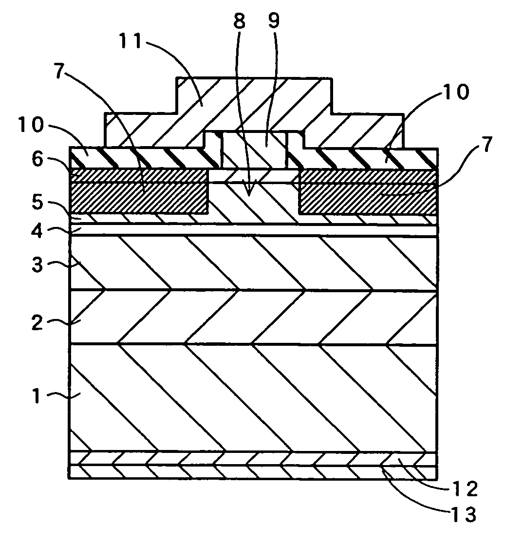
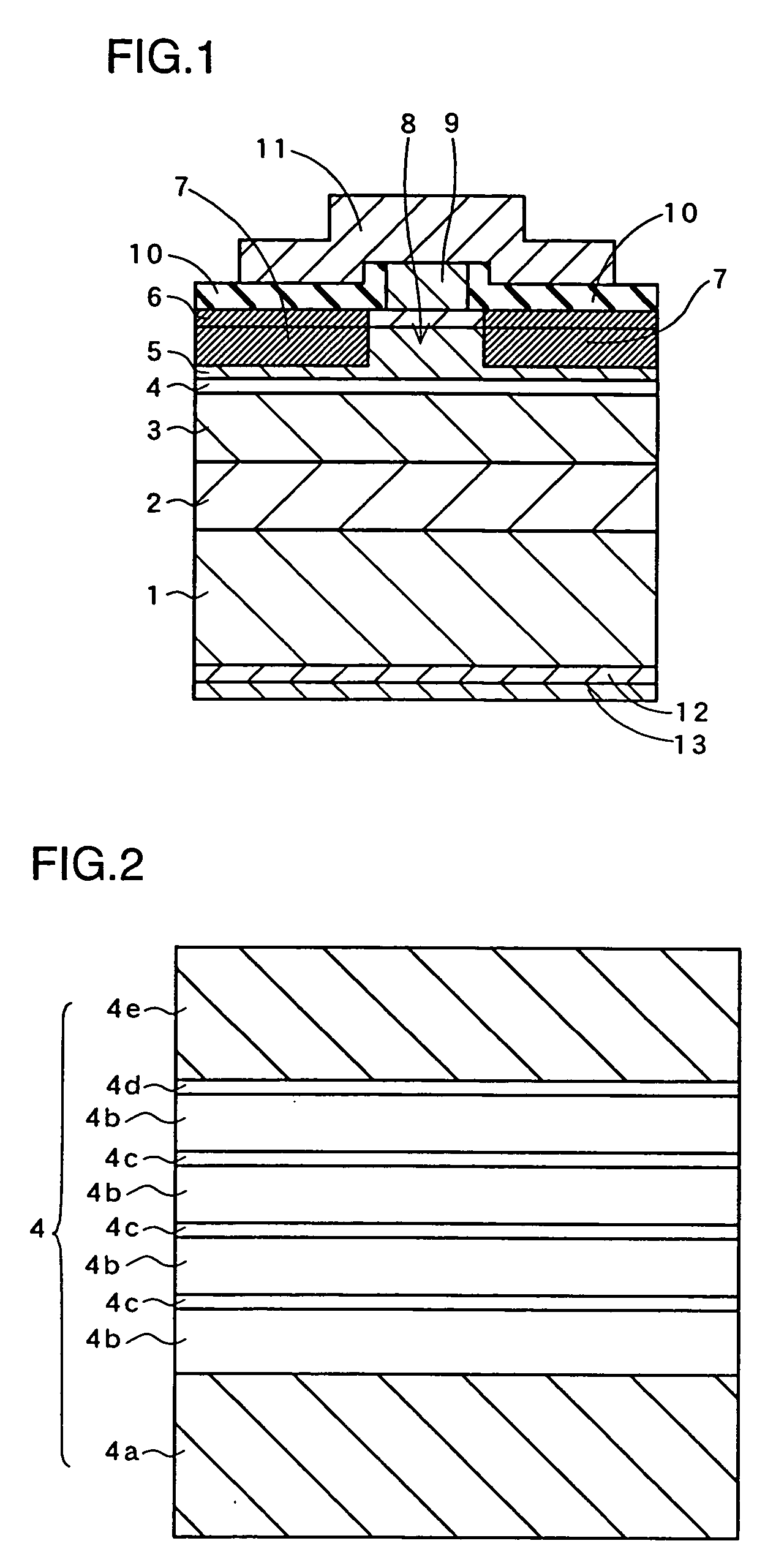
[0377] Referring to FIG. 44, an n-type layer 2, an n-type cladding layer 3, an MQW emission layer 4, a p-type cladding layer 5 and a p-type contact layer 6 are formed on an n-type GaN substrate 1 in this order according to this tenth embodiment, similarly to the first embodiment.

[0378] According to the tenth embodiment, silicon is ion-implanted into partial regions of the p-type cladding layer 5 and the p-type contact layer 6, thereby forming current narrowing layers 97a having a thickness (implantation depth) of...

eleventh embodiment

[0390] Referring to FIG. 47, an example of forming current narrowing layers by thermal diffusion of hydrogen atoms while forming light absorption layers by ion implantation of silicon is described with reference to this eleventh embodiment. In a nitride semiconductor laser element according to this eleventh embodiment, the current narrowing layers are formed over an n-type cladding layer, an MQW emission layer, a p-type cladding layer and a p-type contact layer. The remaining structure of the eleventh embodiment is similar to that of the first embodiment.

[0391] Referring to FIG. 47, an n-type layer 2, an n-type cladding layer 3, an MQW emission layer 4, a p-type cladding layer 5 and a p-type contact layer 6 are formed on an n-type GaN substrate 1 in this order according to this eleventh embodiment, similarly to the first embodiment.

[0392] According to the eleventh embodiment, current narrowing layers107a formed by thermally diffusing hydrogen are formed on partial regions of the p...

twelfth embodiment

[0404] Referring to FIG. 52, a case of forming current narrowing layers and light absorption layers extending over an n-type cladding layer, an MQW emission layer, a p-type cladding layer and a p-type contact layer by ion-implanting silicon twice respectively is described with reference to this twelfth embodiment. The remaining structure of the twelfth embodiment is similar to that of the first embodiment.

[0405] Referring to FIG. 52, an n-type layer 2, an n-type cladding layer 3, an MQW emission layer 4, a p-type cladding layer 5 and a p-type contact layer 6 are formed on an n-type GaN substrate 1 in this order according to this twelfth embodiment, similarly to the first embodiment.

[0406] According to the twelfth embodiment, silicon (Si) is ion-implanted into partial regions of the layers from the n-type cladding layer 3 to the p-type contact layer 6 thereby forming current narrowing layers 117b having a thickness (implantation depth) of about 0.73 μm over the n-type cladding laye...


PUM


Abstract

A nitride semiconductor laser element capable of controlling the lateral confinement of light with a good reproducibility, the nitride semiconductor element comprising an n-type cladding layer (3), an MQW light emitting layer (4) formed on the cladding layer (3), a p-type cladding layer (5) and a p-type contact layer (6) formed on the light emitting layer (4), and an ion implantation light absorbing layer (7) formed, by introducing carbon, in regions other than a current passing region (8) in the cladding layer (5) and the contact layer (6).

Description

TECHNICAL FIELD [0001] The present invention relates to a nitride semiconductor laser element, and more particularly, it relates to a nitride semiconductor laser element having a light absorption layer. BACKGROUND TECHNIQUE [0002] A nitride semiconductor laser element has recently been expected for utilization as the light source for an advanced large capacity optical disk, and is increasingly subjected to development. [0003]FIG. 173 is a sectional view showing the structure of a conventional nitride semiconductor laser element. The structure of the conventional semiconductor laser element is described with reference to FIG. 173. In this conventional nitride semiconductor laser element, an n-type contact layer 1002 of n-type GaN, an n-type cladding layer 1003 of n-type AlGaN, an MQW (Multiple Quantum Well: multiple quantum well) active layer 1004 of InGaN and a p-type cladding layer 1005 having a projecting portion and consisting of p-type AlGaN are formed on a sapphire substrate 10...

Claims


Application Information

Patent Timeline
Patent Type & Authority Applications(United States)
IPC IPC(8): H01L27/10H01S5/22H01S5/323
CPCH01S5/22H01S5/32341H01S5/2219
Inventor TODA, TADAOYAMAGUCHI, TSUTOMUHATA, MASAYUKINOMURA, YASUHIKOSHOUNO, MASAYUKIHISHIDA, YUUJIYODOSHI, KEIICHIINOUE, DAIJIROKANO, TAKASHIHAYASHI, NOBUHIKO
Owner SANYO ELECTRIC CO LTD
Why Eureka
Try Eureka