
Wafer-level assembly method for semiconductor devices

a technology of semiconductor devices and assembly methods, applied in semiconductor devices, semiconductor/solid-state device details, electrical devices, etc., can solve the problems of reducing the efficiency of wafer-level processing, reducing the cost savings of mass processing, and reducing the cost of mass processing. , the effect of reducing the cost of mass processing

Inactive Publication Date: 2006-01-19
GILLEO KENNETH B
View PDF5 Cites 33 Cited by
  • Summary
  • Abstract
  • Description
  • Claims
  • Application Information

AI Technical Summary

Benefits of technology

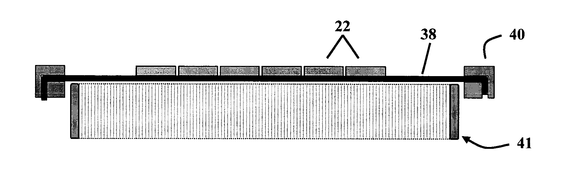
[0017] The expanded carrier that holds the singulated chips can also be bonded to another array of singulated chips affixed to conventional dicing tape. The wafers to be bonded can thus contain chips of different sizes. The elastomeric carrier is expanded until the desired spacing is obtained and then the two arrays of chips are bonded together using solder, adhesive paste, or film. The smaller chip can therefore be bonded to the larger chip so that the connection points, or bond pads, of the larger chip are not obscured by the smaller. This chip-to-chip configuration thus becomes the basis for stacked die multichip modules using ordinary wafers. The advantage is that a large number of chips are simultaneously bonded together instead of one at a time as is presently done. The process can be repeated so that a third chip is added to the stack. The stacking process can be repeated with progressively smaller chips until the desired die stack is achieved. The die stack is now ready to be bonded to a package by applying a die attach adhesive to the bottom die or to the package platform. The stack of die is then interconnected to the package by wire bonding. This process can thus produce the same multichip package products, now manufactured, with minimum labor compared to existing methods where die are singulated and individually stacked.

Problems solved by technology

However, one major limit for this form of processing is that the package size must match physical dimensions of the chip; the package platform must be chip-size.
The size restriction is also a problem for stacked die multichip packaging.
While this allows chips to be stacked, one on top of the other, the many benefits of wafer-level processing is lost.
A limited amount of prior art does describe stacking of chips at wafer-level.
This concept limits the die stack to only two chips and requires complex packaging constructions to connect the chips that are positioned upward and downward.
But all of these methods require added steps to the semiconductor process at a cost penalty.
None of these patents discloses the concept of increasing the spacing between smaller die for bonding to facilitate bonding to larger die by expanding an elastomeric wafer carrier tape.
Even a patent that utilize expandable wafer tape failed to discover the concept of increasing spaces between individual die for stacking.

Method used


Image

  • Wafer-level assembly method for semiconductor devices
  • Wafer-level assembly method for semiconductor devices
  • Wafer-level assembly method for semiconductor devices

Examples


Embodiment Construction

[0041] Described, infra, are novel wafer-level processes that can be used to economically manufacture chip assemblies for multichip modules, component packages, and chip-on-board products. These methods enable semiconductor chips to be simultaneously bonded to a plurality of single chip packages. The method can also be used to pre-assemble chips into a die stack prior to assembling them in a multichip package or module. The method can also be used to simultaneously bond chips to printed circuit boards to greatly reduce manufacturing cost. This can be especially advantageous for producing radio frequency identification products, such as RFID tags, that are extremely cost-sensitive. Unlike prior wafer-level processes, my method allows a plurality of chips to be simultaneously bonded to an array of chips, to packages, or to printed circuit boards. Furthermore, a wafer comprising a plurality of chips can be assembled to other chips, packages, circuits, and the like, that have greater di...


PUM


Abstract

A wafer-level assembly method for bonding chips to other wafers or to arrays of circuits. The method allows an array of chips, held on a temporary carrier, to be separated by expanding said carrier so that said chips can be aligned and bonded to a substrate with dimensions that would not otherwise permit registration of the chips.

Description

RELATED APPLICATIONS [0001] This application claims the benefit of the following: U.S. Provisional Application No. US60 / 587,588 filed Jul. 14, 2004. The entire teachings of this patent application are incorporated herein by reference.FIELD OF INVENTION [0002] The present invention relates to a novel wafer-level assembly method for simultaneously joining all of the integrated circuits contained in a wafer to devices on a second wafer, that can have dissimilar dimensions, to form die stacks useful for multichip modules, and in addition, allows an entire wafer of flip chips to be assembled to an array of printed circuits including, but not limited to, RFID tags. BACKGROUND OF THE INVENTION [0003] Electronic semiconductor chips, or die, (devices for logic functions, memory, radio frequency, optoelectronics, etc.) are generally placed in component packages that are subsequently bonded to printed wiring boards for electronic communication therewith. Electronic packages by providing in sev...

Claims


Application Information

Patent Timeline
IPC IPC(8): H01L23/02
CPCH01L21/6835H01L2924/07811H01L24/81H01L24/97H01L25/0657H01L25/50H01L2221/68327H01L2221/68336H01L2221/68354H01L2224/16145H01L2224/16225H01L2224/32145H01L2224/32225H01L2224/48091H01L2224/48227H01L2224/48247H01L2224/73204H01L2224/73265H01L2224/81001H01L2224/97H01L2924/01013H01L2924/01029H01L2924/01047H01L2924/15311H01L2924/18161H01L21/6836H01L2225/06568H01L2924/014H01L2924/01006H01L2924/01005H01L2224/81H01L2924/00014H01L2924/00H01L2924/00012H01L24/73H01L2224/0554H01L2224/05572H01L2224/05573H01L2924/14H01L2924/181H01L2224/05599H01L2224/0555H01L2224/0556
Inventor GILLEO, KENNETH B.
Owner GILLEO KENNETH B
Learn More