Organic electroluminescent display device

Inactive Publication Date: 2006-01-19
SANYO ELECTRIC CO LTD
View PDF13 Cites 228 Cited by
  • Summary
  • Abstract
  • Description
  • Claims
  • Application Information

AI Technical Summary

Benefits of technology

[0020] As an alternative, a photosensor is disposed in each of the light emitting pixels and comprises a photosensor transistor. The gate of the photosensor transistor receives a constant voltage, the source or the drain of the photosensor trans

Problems solved by technology

Especially, as described above, it is problematic that there are many cases where the unevenness of brightness becomes remarkable among the organic-EL elements, which are current-driven type light emitting elements to emit light depending on a current flowing between the anode and the cathode.
Moreover, although there is a brightness half-life for the organic EL element, this period

Method used


Image

  • Organic electroluminescent display device
  • Organic electroluminescent display device
  • Organic electroluminescent display device

Examples


first embodiment

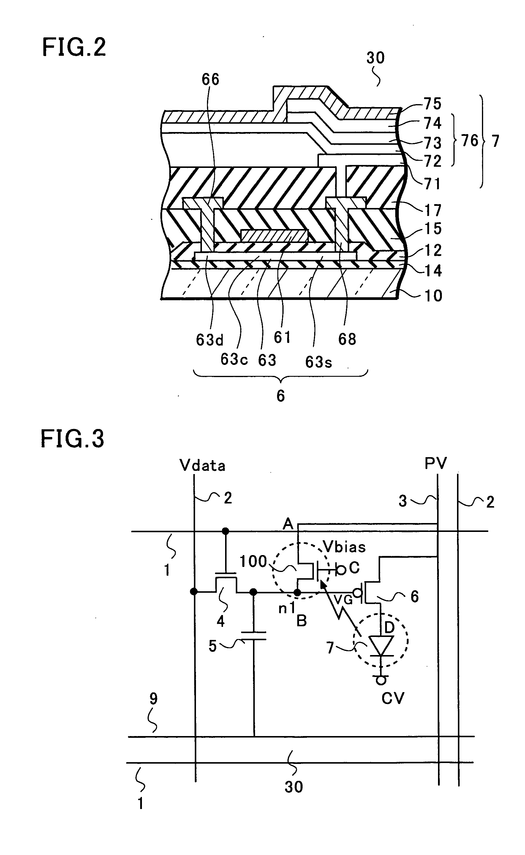
[0043] First, the present invention will be shown in FIGS. 1 to 4B.

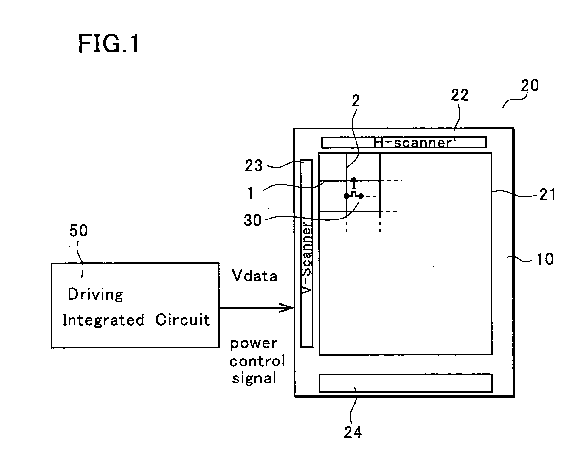
[0044]FIG. 1 is a schematic view showing an organic EL display device. An organic EL display device 20 includes a substrate 10, drain lines 2, gate lines 1, a display unit 21, a horizontal scanning circuit 22, a vertical scanning circuit 23 and photosensors.

[0045] Furthermore, the organic EL display device 20 includes a driving integrated circuit 50. The driving integrated circuit 50 controls the display device by, for example, outputting a data signal Vdata and applying a drive voltage to a transistor which is connected to an organic EL element of the display unit 21 in order to cause the organic EL element to emit light.

[0046] The display unit 21 is formed in a manner that a plurality of light emitting pixels 30 are disposed in a matrix form on the insulating substrate 10 made of a glass plate or the like. The light emitting pixel 30 includes an EL element having a luminescence layer between an anode and a cathod...

second embodiment

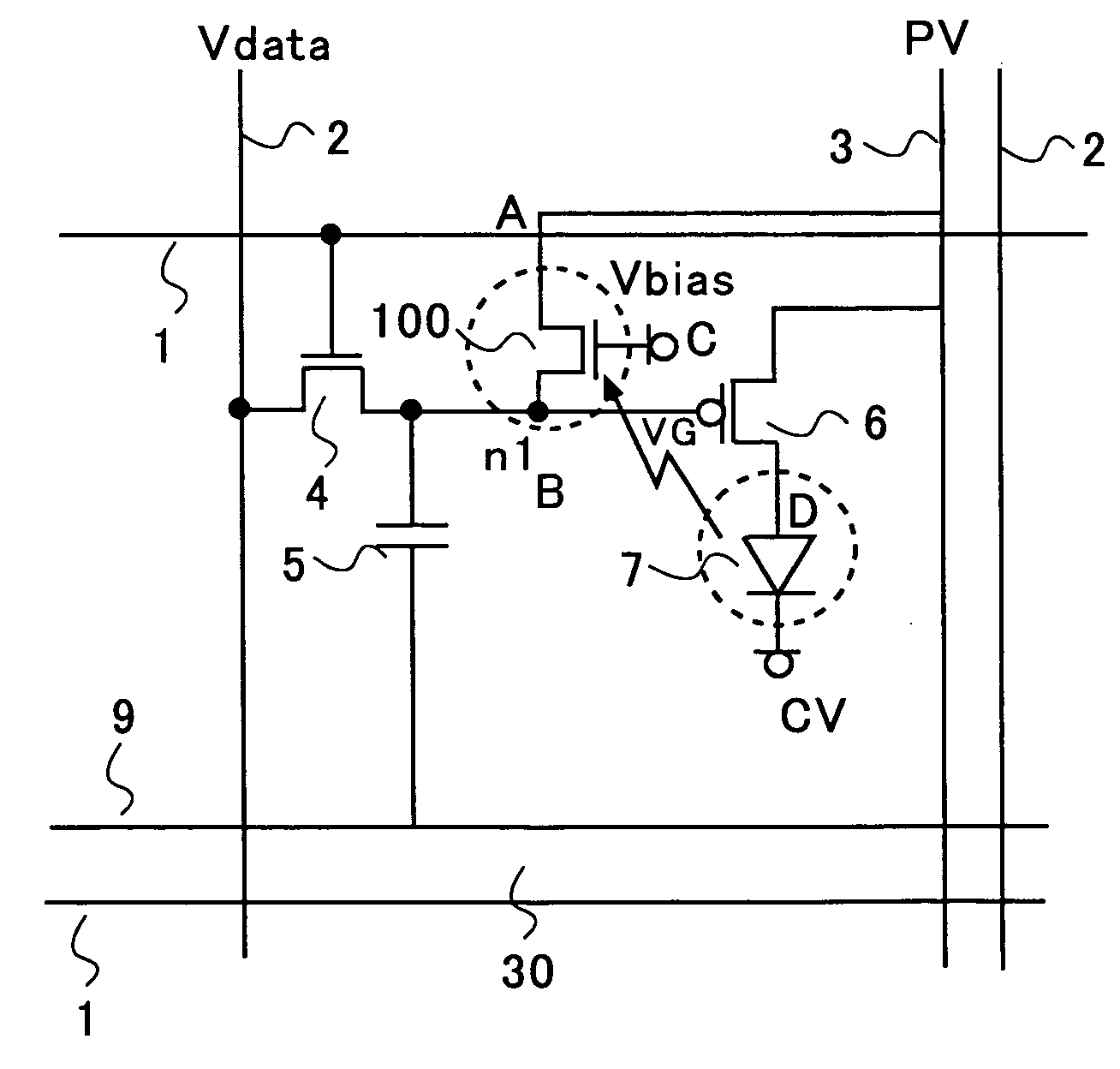
[0088]FIGS. 6A and 6B show one pixel in the FIG. 6A is a circuit diagram. FIG. 6B is a plan view of a circled area shown in FIG. 6A, and terminals A, B, C and D corresponding to those in the circuit diagram of FIG. 6A is shown in FIG. 6B. A cross-sectional view taken along the Y-Y line in FIG. 6B is the same as the one in FIG. 4B. A description thereof will be thus omitted. FIG. 6B is a plan view of when viewed from a substrate 10 side.

[0089] The light emitting pixel 30 is configured to connect a photoreceptor circuit 200, which becomes a photosensor, to a light emitting circuit 180. On the substrate, a plurality of gate lines 1 extending in the row direction are disposed. A plurality of drain lines 2 and first power supply lines 3 extending in the column direction are disposed to intersect the gate lines 1. The first power supply lines 3 are connected to a power source PV. The power source PV is a power source to output a positive constant voltage, for example.

[0090] The light em...


PUM


Abstract

A photosensor is disposed in each pixel, and the brightness is adjusted for each pixel depending on the light quantity of an organic EL element. The adjustment of brightness is realized by making the current amount of a pixel with a high brightness small in accordance with a pixel with a small light emission amount. Thus, low power consumption can be achieved, and the unevenness of brightness can be corrected. By disposing the photosensor to configure a photoreceptor circuit in each pixel, the unevenness of brightness is corrected. Further, it becomes possible to correct brightness in a brightness half-life. Hence, a longer lifetime can be achieved.

Description

BACKGROUND OF THE INVENTION [0001] 1. Field of the Invention [0002] The present invention relates to an organic electroluminescent (EL) display device, particularly to an organic EL display device capable of adjusting the unevenness of brightness in each pixel in a display unit. [0003] 2. Description of the Related Art [0004] Since an organic EL element is self-luminous, a backlight necessary for a liquid crystal display device is not required. Thus, it is optimal to make the display device thinner. In addition, the organic EL element has no limit to a viewing angle. Therefore, the organic EL element is largely expected to become commercially practical as a display device of the next generation. [0005] Incidentally, there are two kinds of drive methods of the organic EL display device: a passive type of a simple matrix and an active type using TFTs. In the active type, a circuit configuration shown in FIG. 15A is generally used. FIG. 15A is a circuit schematic diagram of a display u...

Claims


Application Information

Patent Timeline
IPC IPC(8): G09G3/10G09G3/36
CPCG09G3/3233G09G3/3291G09G2300/0842G09G2300/0852G09G2320/0276G09G2320/0295H01L27/3269G09G2320/045G09G2320/0666G09G2330/021G09G2360/145G09G2360/148G09G2320/043H10K59/13G09G3/30H05B33/26
Inventor OGAWA, TAKASHI
Owner SANYO ELECTRIC CO LTD
Why Eureka
Try Eureka