

Radio tag antenna structure for an optical recording medium and a case for an optical recording medium with a radio tag antenna
- Summary
- Abstract
- Description
- Claims
- Application Information
AI Technical Summary
Benefits of technology
Problems solved by technology
Method used
Image

Examples
first embodiment
(A) Description of First Embodiment
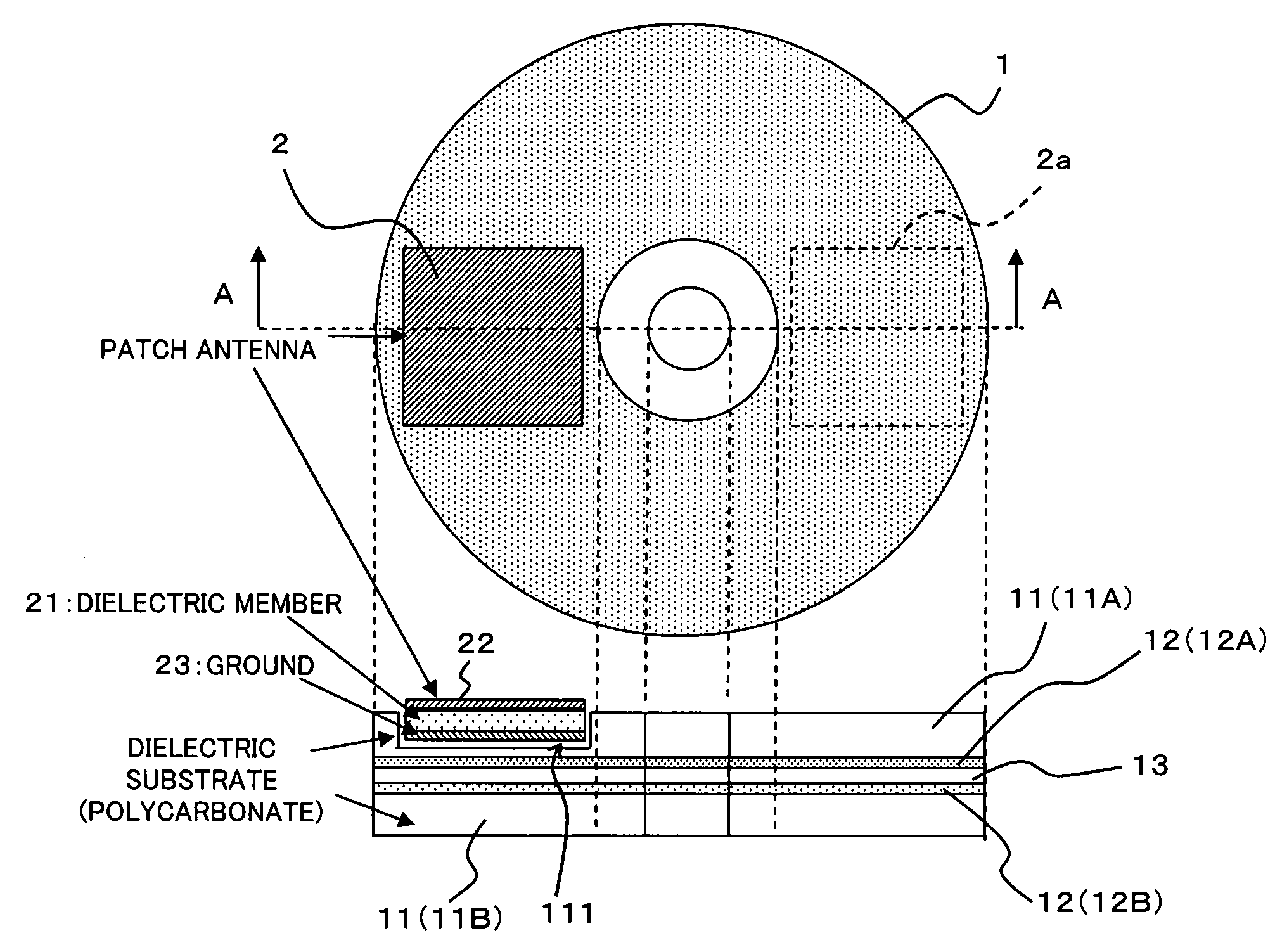
[0063] FIGS. 1(A) and 1(B) are diagrams each showing a radio tag antenna structure for an optical recording medium according to a first embodiment of this invention. FIG. 1(A) is a schematic plan view of a DVD (Digital Versatile Disk) as being an optical recording disk medium, and FIG. 1(B) is a schematic sectional view taken along line A-A of the DVD shown in FIG. 1(A).
[0064] As shown in FIGS. 1(A) and 1(B), the DVD 1 has apparently a similar structure to a CD (Compact Disk). The DVD 1 is generally formed by laminating two disks with an adhesive, each of which has a size according to the standardized specification [for example, an inside diameter of 1.5 cm, an outside diameter of 12 cm (diameter), a thickness of 0.6 mm]. Namely, two disks each of which has a reflective layer (metal layer) 12 (12A, 12B) functioning as a light-reflecting surface formed on one side of a dielectric substrate (dielectric layer) 11 (11A, 11B) are laminated with an adhe...
second embodiment
(B) Description of Second Embodiment
[0098] FIGS. 7(A) and 7(B) are diagrams for illustrating a radio tag antenna structure for an optical recording medium according to a second embodiment of this invention. FIG. 7(A) is a schematic plan view of a CD as being an optical recording disk medium, whereas 7(B) is a schematic sectional view taken along line A-A of the CD shown in FIG. 7(A).
[0099] As shown in FIGS. 7(A) and 7(B), the CD 3 is sized to have an inside diameter of 1.5 cm, an outside diameter (diameter) of 12 cm and a thickness of 0.6 mm. Generally, a reflective layer (metal layer) 12 is formed on one surface of a dielectric substrate (dielectric layer) 11, and a protective layer 14 is further formed thereon, as shown in FIG. 7(B). In FIGS. 7(A) and 7(B), illustration of a recording layer on which information is recorded is omitted.
[0100] In this embodiment, the dielectric substrate 11 also functions as a protective layer for protecting the reflective layer 12 and the recordin...
PUM
 Abstract
Description
Claims
Application Information