Semiconductor device, display apparatus, and display apparatus driving method

a technology of display apparatus and semiconductor device, applied in the direction of static indicating device, identification means, instruments, etc., can solve the problems of difficult to incorporate such a circuit into compact high definition display or the like, and the luminance of the circuit is likely to vary, so as to achieve the effect of low aperture ratio, easy to achieve, and low cos

Active Publication Date: 2006-01-19
SANYO ELECTRIC CO LTD
View PDF3 Cites 22 Cited by
  • Summary
  • Abstract
  • Description
  • Claims
  • Application Information

AI Technical Summary

Benefits of technology

[0023] According to the present invention, an element to be driven can be reliably driven using a minimum number of circuit elements and wires. Therefore, the area occupied by circuit elements and the like in one pixel area can be minimized, and, even for use in a compact display or a high resolution display, in which each pixel has a small area, it is easy to achieve a display accomplishing a high aperture ratio and having an excellent display quality.
[0024] Further, because all transistors can be formed using the same type of transistors, such as n-channel type transistors, and all transistors included in one pixel circuit can be formed in the same process, it is possible to reduce the number of processes. As a result, the present invention is also effective in reducing variations in characteristics.

Problems solved by technology

Therefore, in such cases, variations in luminance are likely to occur.
As a result, because the above-described circuit has a limit to how much the area of each pixel can be reduced, it is difficult to incorporate such a circuit into a compact high definition display or the like, such as an EVF (electronic view finder), in which each pixel has a small area.

Method used


Image

  • Semiconductor device, display apparatus, and display apparatus driving method
  • Semiconductor device, display apparatus, and display apparatus driving method
  • Semiconductor device, display apparatus, and display apparatus driving method

Examples


Embodiment Construction

[0032] A preferred embodiment (hereinafter, referred to as an “embodiment”) of the present invention will be described with reference to the drawings.

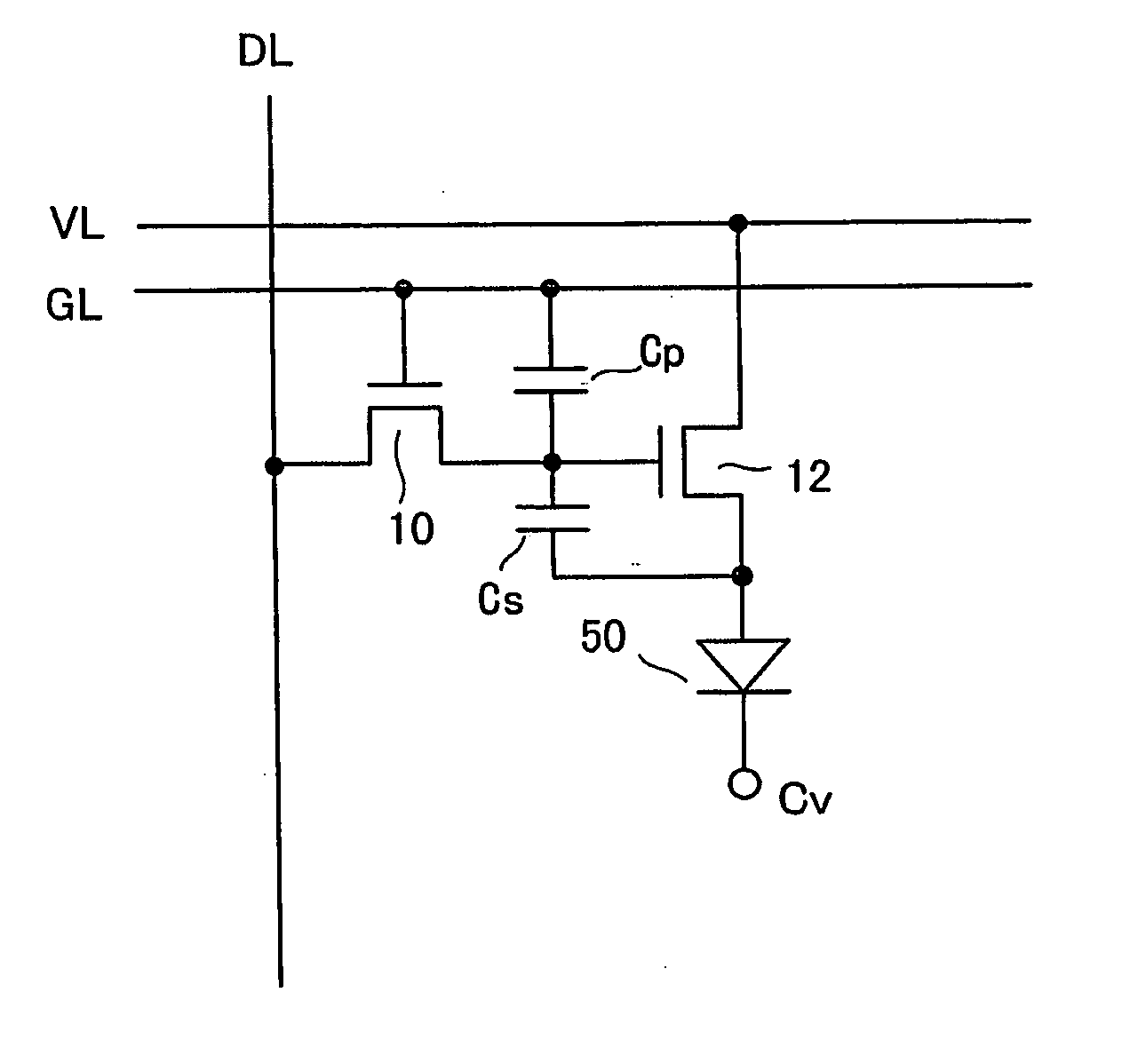
[0033]FIG. 3 shows a circuit structure for one unit of a semiconductor device according to the embodiment of the present invention, and FIG. 4 is a schematic diagram showing an overall structure of a display in which the circuit structure shown in FIG. 3 is used for each pixel. Specifically, the display used in this embodiment is an active matrix type organic EL display that has a plurality of pixels arranged in the form of a matrix on a panel substrate. On this panel substrate, selection lines GL and power supply lines VL are formed in the direction of rows in the matrix, and data lines DL are formed in the direction of columns in the matrix. A selection signal is sequentially output to a selection line GL, a power supply line VL is used to periodically supply operating power (Pvdd) to an element to be driven, and a data signal is ou...


PUM


Abstract

Each of pixels arranged in a matrix comprises an element to be driven, a switching TFT, an element driving TFT, and a storage capacitor, and a potential shifting capacitor. The storage capacitor is connected between the gate and a source of the element driving TFT. Before a data signal is output, a precharge signal is output to a data line to turn on the element driving TFT, a set signal is output to a power supply line that is used to supply power through the turned-on element driving TFT to the element to be driven, and, before a data signal is applied to one electrode of the storage capacitor, the source of the element driving TFT and another electrode of the storage capacitor are discharged in response to the set signal to be fixed at a constant potential. By performing control as described above, the element to be driven is driven using a minimum number of circuit elements.

Description

CROSS-REFERENCE TO RELATED APPLICATIONS [0001] The entire disclosure of Japanese Patent Application Nos. 2004-210729 and 2005-199419 including specification, claims, drawings, and abstract is incorporated herein by reference. BACKGROUND OF THE INVENTION [0002] 1. Field of the Invention [0003] The present invention relates to a circuit structure for controlling an element to be driven, such as an electroluminescence display element. [0004] 2. Description of the Related Art [0005] Because electroluminescence displays that use a self-emitting electroluminescence (hereinafter, referred to as “EL”) element for each pixel as an emissive element are of a self light emitting type, and have advantages such as that the displays are thin and have low power consumption, a great deal of attention has come to be focused on such EL displays, and research is being conducted to use such EL displays as substitutes for displays such as liquid crystal displays (LCDs) or CRTs. [0006] Among various types...

Claims


Application Information

Patent Timeline
Patent Type & Authority Applications(United States)
IPC IPC(8): G09G3/30
CPCG09G3/3233G09G3/3291G09G2320/0238G09G2300/0866G09G2310/0248G09G2300/0852G09F9/30G09G3/30
Inventor IKEDA, KYOJI
Owner SANYO ELECTRIC CO LTD
Why Eureka
Try Eureka