Method and apparatus for providing shear-induced alignment of nanostructure in thin films

a technology of nanostructure and thin film, applied in photomechanical equipment, instruments, coatings, etc., can solve the problems of inability to accurately and consistently align nanostructures in thin films, lack of order, and thus addressability, and limit data storage density to well below the theoretical maximum of one bit per nanodomain

Inactive Publication Date: 2006-01-19
THE TRUSTEES FOR PRINCETON UNIV
View PDF8 Cites 76 Cited by
  • Summary
  • Abstract
  • Description
  • Claims
  • Application Information

AI Technical Summary

Benefits of technology

[0011] The present invention also provides an apparatus for aligning nanostructures in thin films. The apparatus comprises a substrate for receiving a thin film containing nanostructures to be aligned; means for annealing the thin film; and means for imparting a shear stress on the thin film. The means for imparting a shear stress comprises, in one embodiment of the present invention, a flexible or rigid pad positioned on the thin film and means for moving the pad with respect to the substrate. A weight could be placed on the pad to ensure uniform contact between the pad and the thin film. In another embodiment of the present invention, a thin fluid layer is provided between the pad and the thin film, wherein shear stress is transmitted through the thin fluid layer to the thin film. The fluid layer could comprise a viscous silicone, hydrocarbon oil, or other suitable fluid. Optionally, the pad and weight could be replaced with a rolling apparatus, and shear applied to the thin film using a rolling process to align nanostructures in the film. Further, shear could be applied to the thin film using a confined channel and a fluid flowing through the channel.

Problems solved by technology

A significant shortcoming with existing template fabrication techniques is an inability to accurately and consistently align nanostructures in thin films.
This results in a lack of order, and thus addressability, of nanodomains in the film, which limits data storage density to well below the theoretical maximum of one bit per nanodomain.
While the resulting arrays typically display excellent short-range order, due to the existence of topological defects, only limited-range order can be achieved by traditional self-assembly, even when coupled with annealing.
However, the high degree of isotropy imposed by the hexagonal packing of the spherical nanodomains complicates the alignment problem.
For example, electric fields, which are highly successful for in-plane alignment of cylinder-forming BCPs for defining templates of stripe arrays, have not been profitably applied to arrays of BCP spheres.

Method used


Image

  • Method and apparatus for providing shear-induced alignment of nanostructure in thin films
  • Method and apparatus for providing shear-induced alignment of nanostructure in thin films
  • Method and apparatus for providing shear-induced alignment of nanostructure in thin films

Examples


example 1

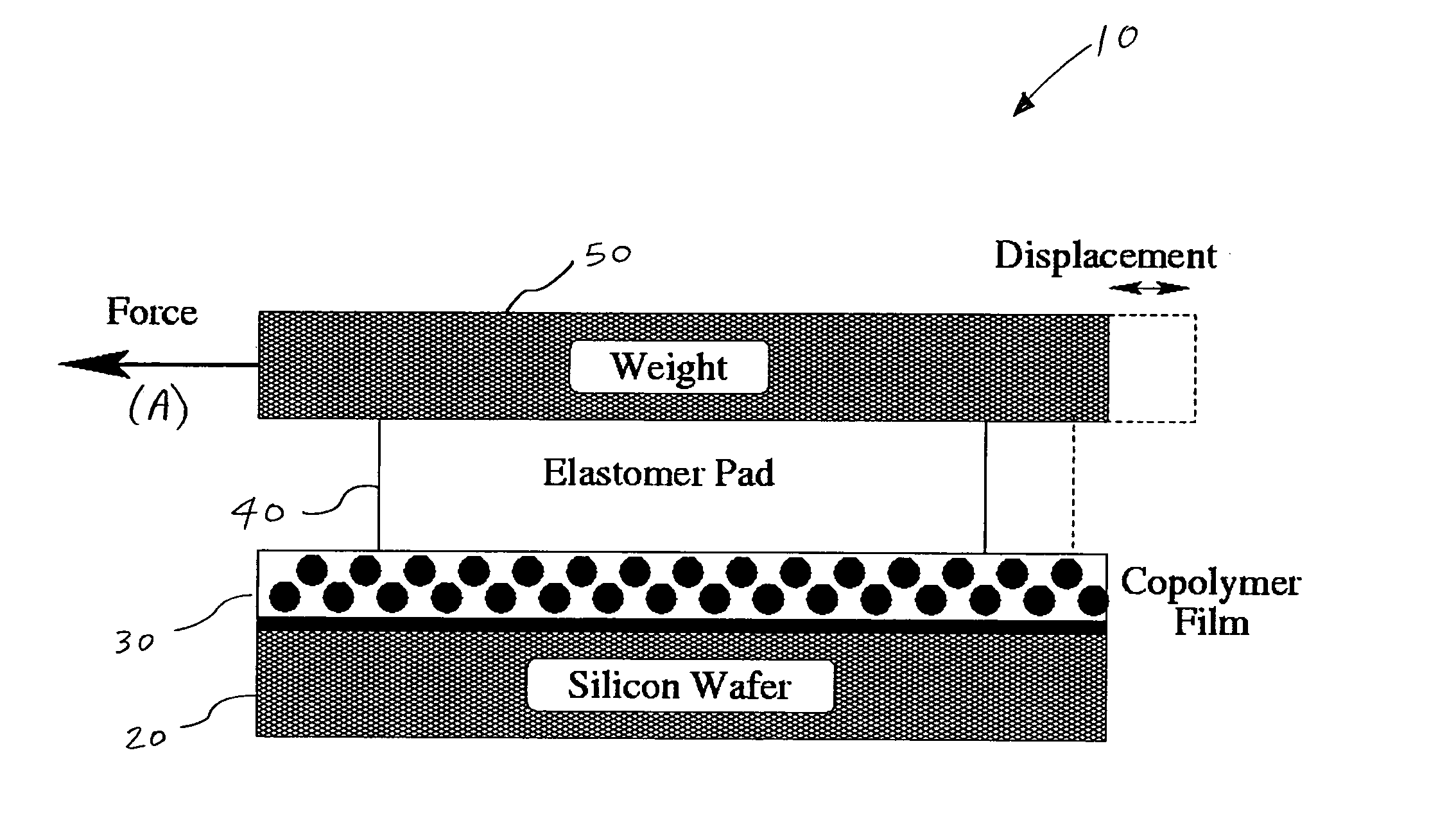
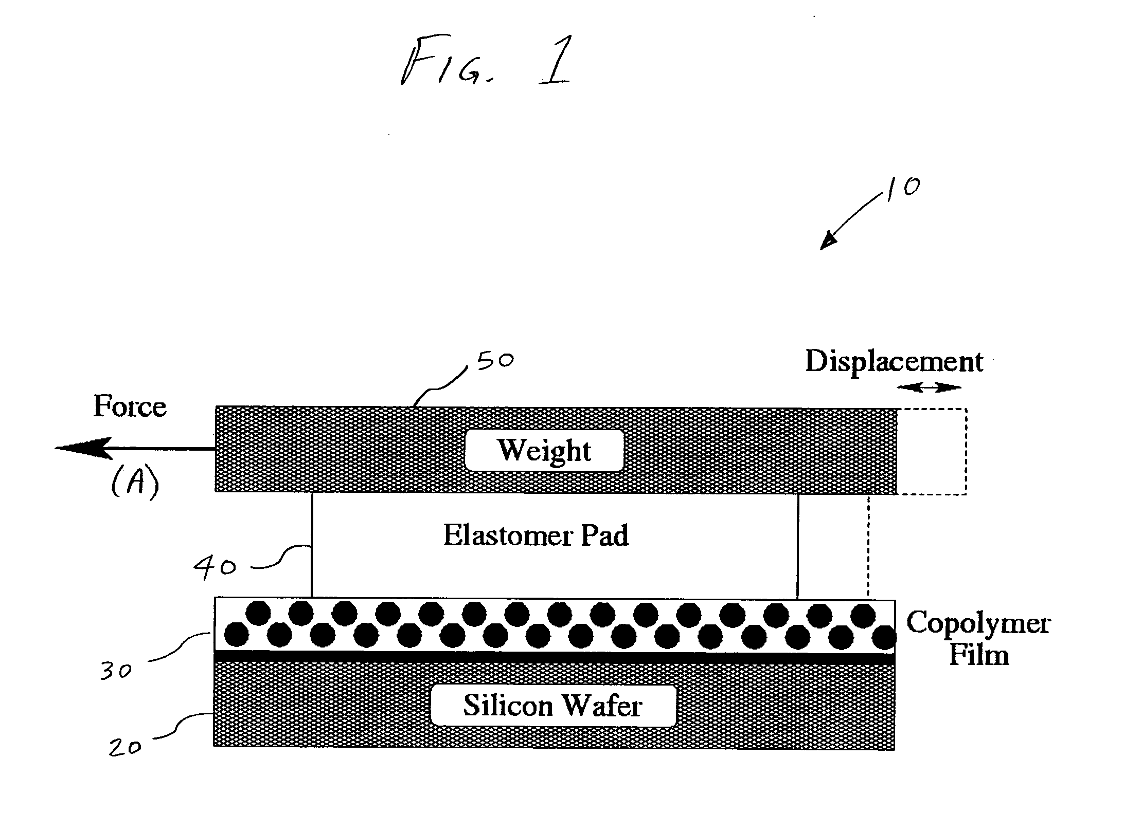
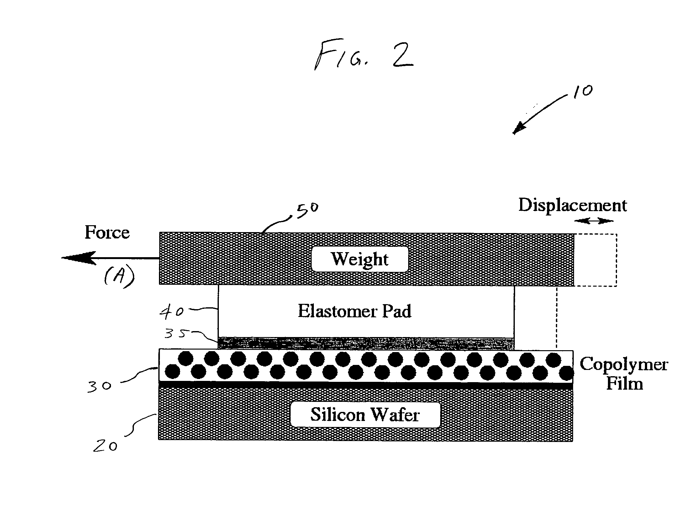
[0030]FIGS. 4a-4b are tapping-mode atomic force microscopy (TM-AFM) images of a sheared PS-PEP 3-23 BCP bilayer film produced by the present invention, taken at two separate locations on a single cm2 sample. The BCP film was approximately 50 nm in thickness, which corresponds to the thickness of two layers of nanodomains. The substrate thickness was approximately 500 microns, and a PDMS pad having a thickness of approximately 1 mm and an area of approximately 1 cm2 was utilized. A shearing force of approximately 0.8 N was applied to the pad, and a weight of approximately 9.8 N was provided on the pad. The sample was heated to a temperature of approximately 100 degrees C., and the BCP layer was sheared for approximately 20 minutes. As can be seen in both images, TM-AFM imaging revealed an aligned hexagonal lattice over the full extent of the sheared region of the BCP layer, with one of the lattice directions coinciding with the shear direction. The inserts in FIGS. 4a-4b show Fourier...

example 2

[0032] As mentioned earlier, the thickness of the BCP layer significantly affects the quality of alignment produced by the present invention. This can be appreciated with reference to FIG. 5, which is a TM-AFM image showing a disordered BCP bilayer film resulting from shear stress applied to slightly thicker and thinner films, as well as monolayer films. The BCP film was approximately 49 nm in thickness. The substrate thickness was approximately 500 microns, and a PDMS pad having a thickness of approximately 1 mm and an area of approximately 1 cm2 was utilized. A shearing force of approximately 0.8 N was applied to the pad, and a weight of approximately 9.8 N was provided on the pad. The sample was heated to a temperature of approximately 100 degrees C., and the BCP layer was sheared for approximately 20 minutes.

[0033] The image of FIG. 5 shows a completely disordered lattice, with no translational or orientational order. The density of topological defects is also very high, with a...

example 3

[0035]FIG. 6 is a scanning electron microscope (SEM) image of an aligned BCP thin film of polyisoprene (PI) spheres in a polystyrene (PS) matrix taken with staining of the film using osmium tetroxide. It has been found that good alignment can be achieved with a PS-PI 68-12 BCP layer having a thickness of 110 nm. At room temperature, PI is a rubber and PS is a glass. The PS-PI 68-12 layer is heated to 180° C., wherein the PI and PS materials are fluids. The PS-PI 68-12 BCP layer is formed on the substrate in similar fashion as the PS-PEP 3-23 BCP layer discussed earlier, and an elastomer pad applied to the PS-PI 68-12 BCP layer. The substrate thickness was approximately 400 microns, and a PDMS pad having a thickness of approximately 1 mm and an area of approximately 1 cm2 was utilized. A shearing force of approximately 0.07 N was applied to the pad, and a weight of approximately 9.8 N was provided on the pad. The sample was heated to a temperature of approximately 180 degrees C., and...


PUM

PropertyMeasurementUnit
thicknessaaaaaaaaaa
thicknessesaaaaaaaaaa
areaaaaaaaaaaa

Abstract

A method and apparatus is disclosed for providing shear-induced alignment of nanostructures, such as spherical nanodomains, self-assembled nanodomains, and particles, in thin films, such as block copolymer (BCP) thin films. A silicon substrate is provided, and a thin film is formed on the substrate. A pad is then applied to the thin film, and optionally, a weight can be positioned on the pad. Optionally, a thin fluid layer can be formed between the pad and the thin film to transmit shear stress to the thin film. The thin film is annealed and the pad slid in a lateral direction with respect to the substrate to impart a shear stress to the thin film during annealing. The shear stress aligns the nanostructures in the thin film. After annealing and application of the shear stress, the pad is removed, and the nanostructures are uniformly aligned.

Description

RELATED APPLICATIONS [0001] This application claims the benefit of U.S. Provisional Application Ser. No. 60 / 563,652 filed Apr. 20, 2004, the entire disclosure of which is expressly incorporated herein by reference.STATEMENT OF GOVERNMENT INTERESTS [0002] The present invention was made under a grant of the National Science Foundation, Grant No. DMR-0213706. Accordingly, the Government may have certain interests in the present invention.BACKGROUND OF THE INVENTION [0003] 1. Field of the Invention [0004] The present invention relates to the alignment of nanostructures in thin films. More specifically, the present invention relates to shear-induced alignment of spherical nanodomains in block copolymer films. [0005] 2. Related Art [0006] Nanofabrication is witnessing a rapid trend towards self-assembled templates as a cost-effective method of generating densely-patterned surfaces. Such surfaces are particularly desirable in forming high-density memory arrays and devices. Templating with ...

Claims


Application Information

Patent Timeline
Patent Type & Authority Applications(United States)
IPC IPC(8): B05D3/02B05D1/40
CPCH01L21/312B82Y30/00G03F7/0002H01L21/02118
Inventor ANGELESCU, DAN E.WALLER, JUDITH H.WU, MINGSHAW W.CHAIKIN, PAUL M.REGISTER, RICHARD A.
Owner THE TRUSTEES FOR PRINCETON UNIV
Why Eureka
Try Eureka