

Resist pattern forming method based on near-field exposure, and substrate processing method and device manufacturing method using the resist pattern forming method
a resist pattern and near-field exposure technology, applied in the field of resist pattern forming method based on near-field exposure, can solve the problems of shortening the wavelength of light source, bulky apparatus, and development of lenses usable in shortened wavelengths, and reducing the cost of resist materials
- Summary
- Abstract
- Description
- Claims
- Application Information
AI Technical Summary
Benefits of technology
Problems solved by technology
Method used
Image

Examples
Embodiment Construction
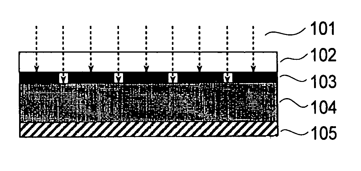
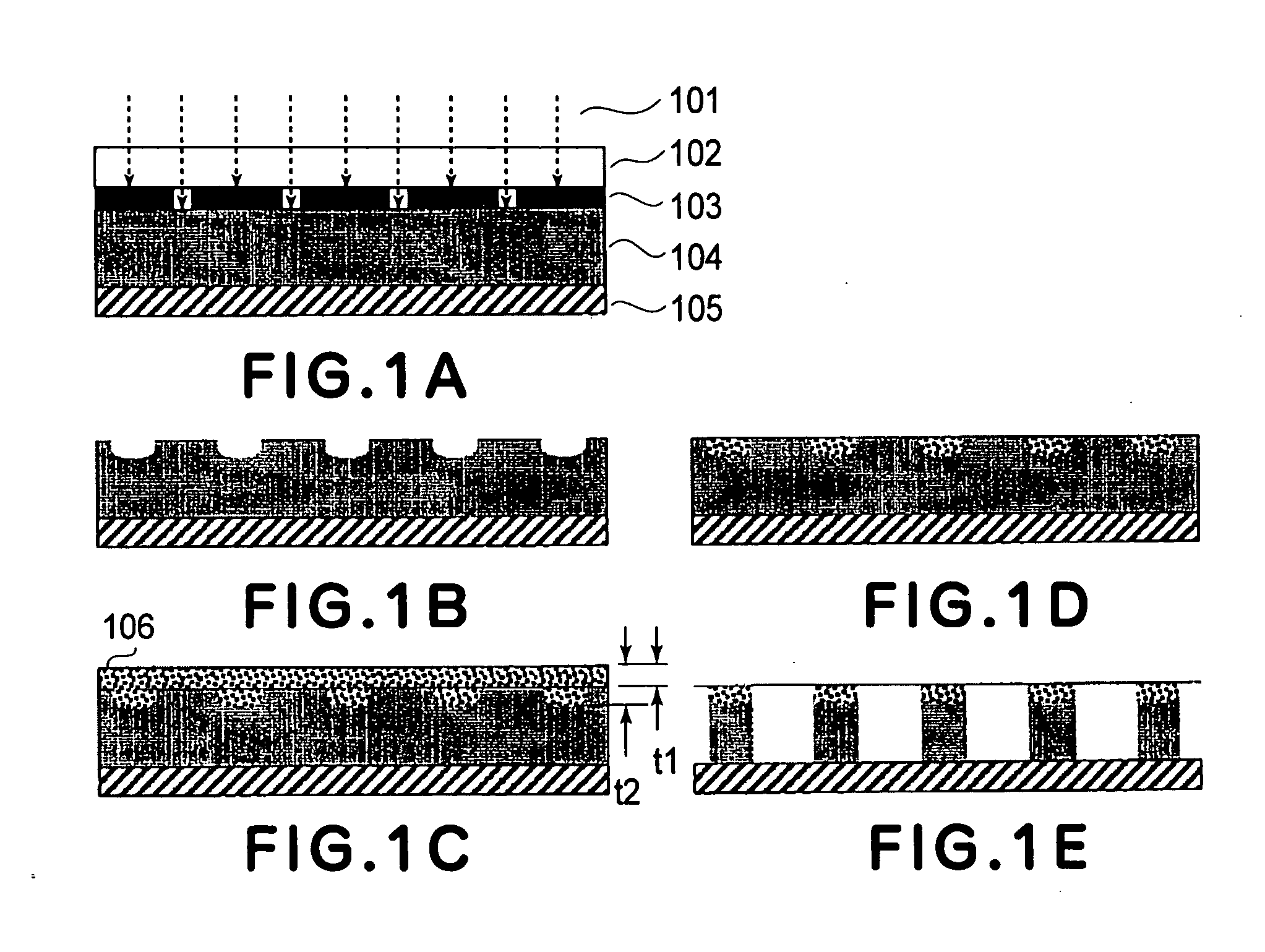
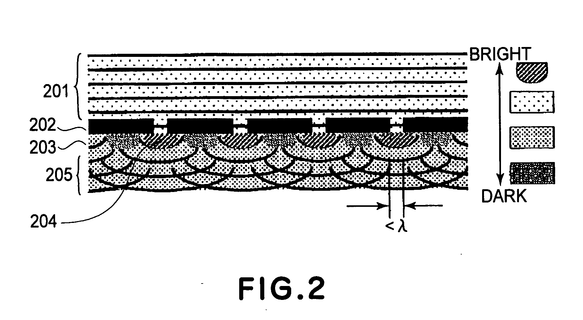
[0017] Preferred embodiments of the present invention, for a resist pattern forming method based on near-field exposure and using a negative type resist, will now be described.
[0018] Initially, as regards a substrate to be processed, a wide variety of materials may be used. Examples are a semiconductor substrate such as Si, GaAs, Inp, etc., an insulative substrate such as glass, quartz, BN, etc., and a substrate made of any one of these materials and having a film thereon being made of one or more of resist, metal, oxide, nitride and the like. As regards a negative type resist material, usable examples are acid catalyst condensation bridge (chemical amplification) type resist, optical cationic polymerization type resist, optical radical polymerization type resist, polyhydroxystyrene-bisazide type resist, cyclized rubber-bisazide type resist, polycinnamic acid vinyl, etc. From the standpoint of sensitivity, acid catalyst condensation bridge type resist is particularly preferable.
[0...
PUM
| Property | Measurement | Unit |
|---|---|---|
| size | aaaaa | aaaaa |
| thickness | aaaaa | aaaaa |
| temperature | aaaaa | aaaaa |
Abstract
Description
Claims
Application Information