Method of Manufacturing A Nano Structure By Etching, Using A Substrate Containing Silicon

a nano-structure and nano-etching technology, applied in nanotechnology, nanoinformatics, electric devices, etc., can solve the problems of difficult to form patterns having a line width half or less than the wavelength of the light source being used, and particularly difficult to form patterns having a line width of 500 nm or less,

Inactive Publication Date: 2011-02-03
CANON KK
View PDF4 Cites 6 Cited by
  • Summary
  • Abstract
  • Description
  • Claims
  • Application Information

AI Technical Summary

Benefits of technology

[0043]According to the present invention, a nano structure formed on the surface of a substrate containing Si and having a pattern of 2 μm or more in depth can be realized.
[0044]Further, the present invention can realize a nano structure having a pattern of 500 nm or less and, particularly, 100 nm or less in line width and 2 μm or more in depth.
[0036]Further, an object of the present invention is to provide a method capable of manufacturing a nano structure having a pattern with a high aspect and a nano order on the substrate containing Si.

Problems solved by technology

In the pattern forming method by this photolithography, a resolving power depends on the wavelength of the light source, and it is particularly difficult to form a pattern having a line width half or less than that of the wavelength of the light source being used.
Consequently, it is difficult to form a pattern having a line width of 500 nm or less by using these light sources.
Further, it is difficult to form a pattern having a line width of 100 nm or less.
In a case in which such a fine pattern is formed, when it is processed up to the depth of, particularly, 2 μm or more, and, particularly, 10 μm or more, maintaining the processing accuracy becomes more difficult.
However, in the pattern forming method by the conventional photolithography, the pattern formation of an extremely fine line width (particularly, 100 nm or less) is difficult.
When the line width is processed up to the depth of, particularly, 2 μm or more, and, particularly, 10 μm or more, maintaining the processing accuracy becomes more difficult.
Hence, the pattern formation by the line width of 500 nm or less, particularly, 100 nm or less, is difficult.
Hence, the change of a condition and the outputting of a condition take time and labor, and, in addition, the etching of the depth of 2 μm or more, and, particularly, 10 μm or more, is difficult.
Further, for the formation of a high aspect step, an application of a higher voltage is required, and therefore, not only is there a limit of the voltage application, but also, as the injection depth becomes deeper, the large lateral spread of the injected ions is produced.
Hence, this is not suitable for the high aspect micro pattern formation.
This makes it difficult to output the condition of the electron beam irradiation with a good positional accuracy.
When these processes are used for electronic devices, the Ga ions are likely to affect the device performance, and a high temperature heating process for stripping the mask material containing Ga and taking out the injected Ga is required.
However, when looking at the ion implanting method of FIG. 21, though this method is configured to deflect ions so as to be irradiated on the substrate, no mention is made of a configuration and an aperture for focusing ions.
In this method, since ions are configured not to be sufficiently focused as compared with the FIB, the patterning of 100 nm or less is difficult if the mask is not used.
Such a method is difficult to obtain a high etching selection ratio with the mask and the etching material, and therefore, it is difficult to form a structure having a depth of 2 μm or more (particularly, 10 μm or more) with good shape control properties.
Particularly, it is difficult to form a high aspect structure, that is, a structure being narrow in width against the depth or the height.
Particularly, this is not suitable for the fine pattern, which requires a deep dig (discussed below) with a width of submicrons (particularly, 500 nm or less) and a depth of 2 μm or more.

Method used


Image

  • Method of Manufacturing A Nano Structure By Etching, Using A Substrate Containing Silicon
  • Method of Manufacturing A Nano Structure By Etching, Using A Substrate Containing Silicon
  • Method of Manufacturing A Nano Structure By Etching, Using A Substrate Containing Silicon

Examples


first embodiment

[0080]Next, a nano structure and a method of manufacturing the nano structure in a first embodiment of the present invention, to which a pattern forming method of the present invention is applied, will be described.

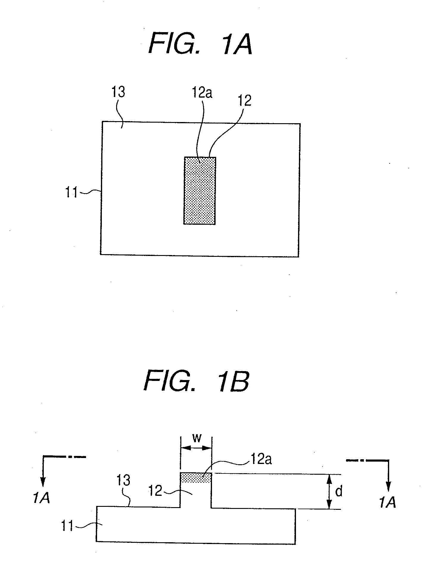
[0081]With reference to FIGS. 1A and 1B, a configuration example of the nano structure having a pattern containing a desired Ga on the surface of a substrate containing Si in the present embodiment will be described. FIG. 1A is a top plan view and FIG. 1B is a sectional view.

[0082]In FIGS. 1A and 1B, reference numeral 11 denotes a substrate, reference numeral 12 denotes a pattern, reference numeral 12a denotes a pattern surface, and reference numeral 13 denotes an etching bottom.

[0083]In the nano structure in the present embodiment, as the substrate 11, a substrate containing Si is used.

[0084]For example, not only a single substrate such as silicon, SiO2, and SiN, but also, a silicon film on SiO2, an SiN film on SiO2, an SiO2 film on silicon, an SiN film on silicon, a sil...

second embodiment

[0131]Next, a method of manufacturing a nano structure for manufacturing the nano structure having a convexo-concave pattern by a predetermined pitch on the substrate surface by etching by using a substrate containing Si in a second embodiment of the present invention will be described.

[0132]FIGS. 5A, 5B, and 5C are views describing a pattern forming method in the present embodiment.

[0133]In FIGS. 5A, 5B, and 5C, reference numeral 21 denotes a substrate containing Si, reference numeral 22 denotes a pattern, reference numeral 22a denotes a pattern surface, reference numeral 23 denotes an etching bottom, reference numeral 24 denotes a focused ion beam (FIB), reference numeral 25 denotes an FIB irradiated area, and reference numeral 26 denotes a reactive ion etching.

[0134]Further, in FIG. 6, one example of the irradiation condition of the focused ion beam (FIB) in the pattern forming method of the present embodiment is illustrated.

[0135]In FIG. 6, to the same regions as the regions sho...

example 1

[0157]In a first example 1, one example of fabricating a nano structure illustrated in FIGS. 1A and 1B will be described.

[0158]As the substrate 11, the Si substrate was used. The pattern width W was taken as 100 nm, and the etching depth was taken as 20 μm.

[0159]Since the manufacturing method of the nano structure in the present example is basically by the same process as the manufacturing method of the nano structure illustrated in FIGS. 4A, 4B, and 4C described in the embodiment of the present invention, a description will be made here by using FIGS. 4A, 4B, and 4C also.

[0160]First, the Si substrate 11 is set to the focused ion beams (FIB) apparatus (FIG. 4A). At that time, the Si substrate 11 is set so as to be vertical to the focus ion beam (FIB) 14. Although the focused ion beam (FIB) 14 is suitably adjusted in advance, before the irradiation, accuracy was confirmed in the substrate edge vicinity.

[0161]Five irradiation areas of 10 μm in length and a width W=100 nm are set in th...


PUM

PropertyMeasurementUnit
depthaaaaaaaaaa
wavelengthaaaaaaaaaa

Abstract

A method of manufacturing a nano structure by etching, using a substrate containing Si. A focused Ga ion or In ion beam is irradiated on the surface of the substrate containing Si. The Ga ions or the In ions are injected while sputtering away the surface of the substrate so that a layer containing Ga or In is formed on the surface of the substrate. Dry etching by a gas containing fluorine (F) is performed with the layer containing the Ga or the In formed on the surface of the substrate taken as an etching mask, and the nano structure is formed having a pattern of at least 2 μm tin in depth according to a predetermined line width.

Description

[0001]This application is a divisional application of copending U.S. patent application Ser. No. 12 / 109,701, filed on Apr. 25, 2008.[0002]This application claims the benefit of Japanese Patent Application No. 2007-128789, filed May 15, 2007, and No. 2008-077106, filed Mar. 25, 2008, which are hereby incorporated by reference herein in their entirety.BACKGROUND OF THE INVENTION[0003]1. Field Of The Invention[0004]The present invention relates to a nano structure and a method of manufacturing a nano structure.[0005]2. Related Background Art[0006]In recent years, accompanied with the high integration of semiconductor integrated circuits, demand has further increased for forming a fine pattern having a high accuracy.[0007]Heretofore, a pattern forming method using photolithography has been used for the formation of a microstructure.[0008]In the pattern formation by this method, a photosensitizing agent, such as a resist, is applied to a substrate to form a resist film, and after that, t...

Claims


Application Information

Patent Timeline
Patent Type & Authority Applications(United States)
IPC IPC(8): H01L21/308
CPCB82Y10/00H01L21/31144H01L21/3083
Inventor MOTOI, TAIKOTAMAMORI, KENJIWANG, SHINANOKUNUKI, MASAHIKOONO, HARUHITOAIBA, TOSHIAKIYOSHIMATSU, NOBUKI
Owner CANON KK
Why Eureka
Try Eureka