Method and structure for strained finfet devices

a technology of finfets and structures, applied in the direction of semiconductor devices, electrical apparatus, transistors, etc., can solve the problems of lowering yield, strained si by sige is even more difficult to implement in finfets, and is difficult to achiev

Active Publication Date: 2006-01-19
GLOBALFOUNDRIES US INC
View PDF16 Cites 138 Cited by
  • Summary
  • Abstract
  • Description
  • Claims
  • Application Information

AI Technical Summary

Benefits of technology

[0014] Thus, the present invention provides an improved method to provide stressed regions within a device, such that each device can be separately tuned to achieve an optimal stressed region.

Problems solved by technology

However, strained Si by SiGe has been challenging to implement, and strained Si by SiGe is even more difficult to implement in FinFETs.
However, conventional methods to strain Si by SiGe to obtain improvement in nFETs cause more defects, thereby lowering yields.
Moreover, it has been very difficult to realize any improvement in pFET performance using the strained Si by the SiGe technique.

Method used


Image

  • Method and structure for strained finfet devices
  • Method and structure for strained finfet devices
  • Method and structure for strained finfet devices

Examples


Embodiment Construction

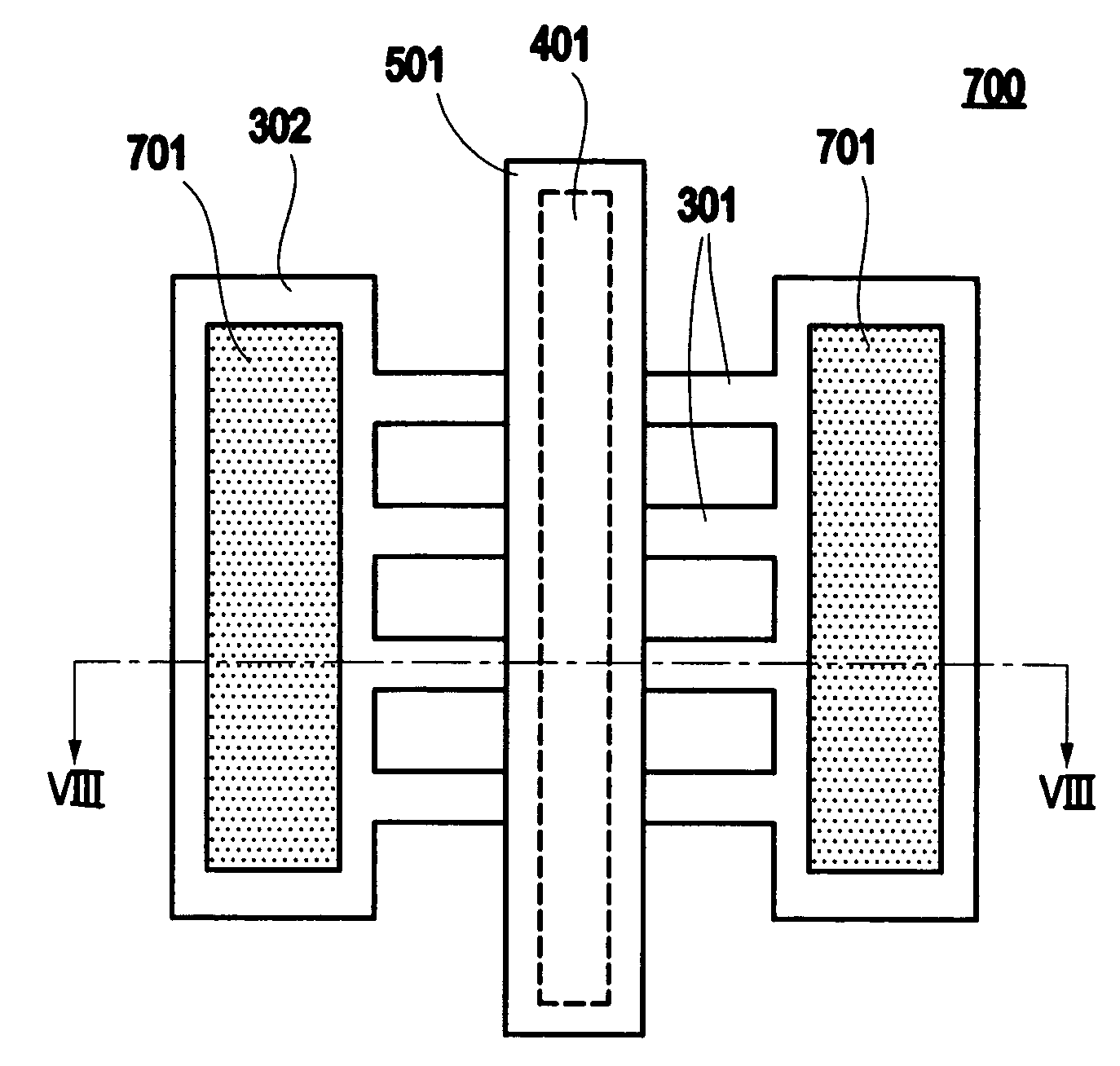
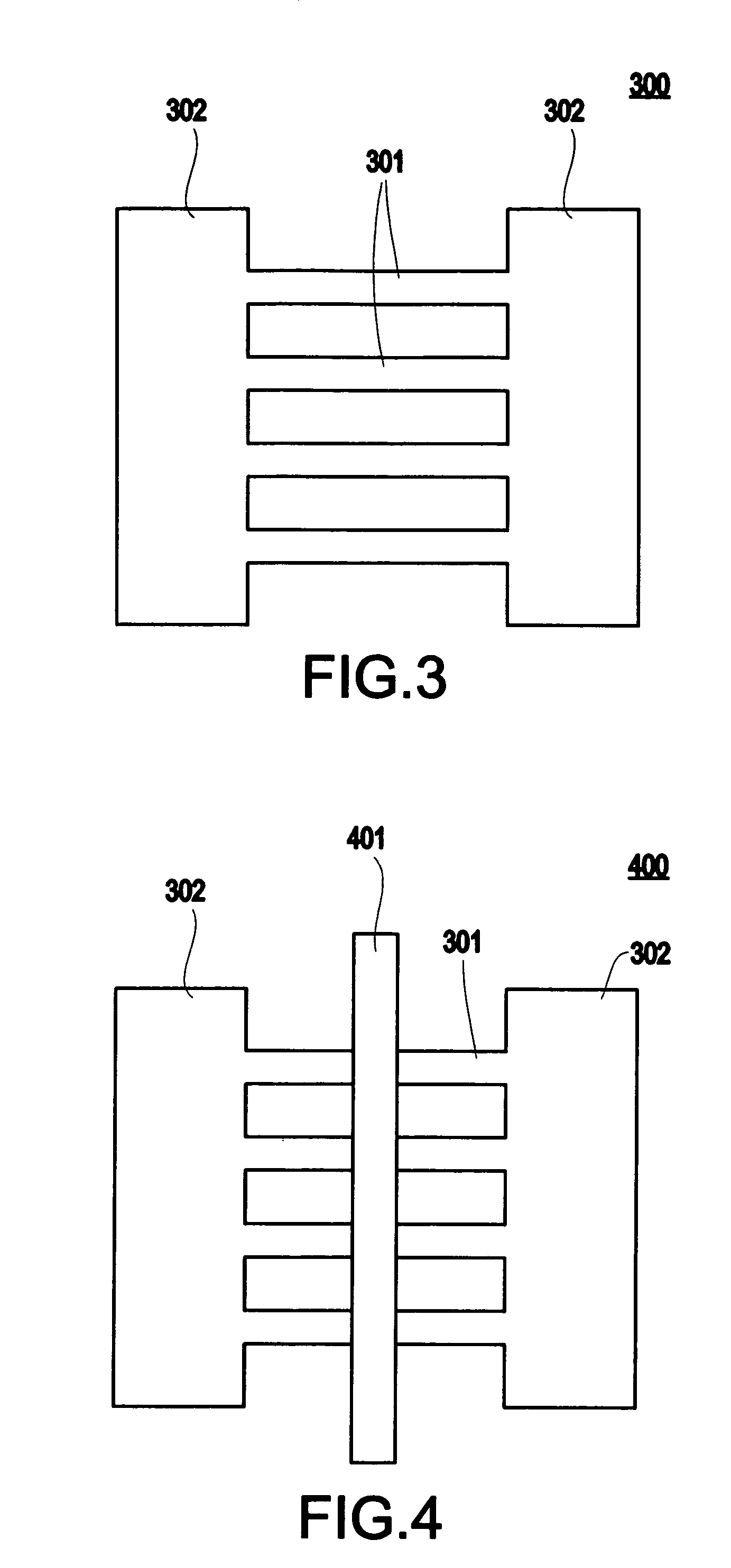
[0026] Referring now to the drawings, and more particularly to FIGS. 3-10, an exemplary embodiment of the present invention will now be described.

[0027] In contrast to conventional techniques, the present invention is directed toward improving performance in FinFETs by using a local mechanical stress. The technique described herein overcomes challenges associated with conventional strained Si by SiGe. The method involves novel process steps to impose channel stress to improve mobility for both n- and p-type Fin channels. In the exemplary embodiment discussed below, the stress is locally created in the Fin connector structures, but it should be apparent to one of ordinary skill in the art, after taking the following discussion as a whole, that this concept is easily generalized to other devices and appropriate locations within these devices.

[0028] A unique aspect of the FinFET is that, since all devices have the same width, FinFET circuits have a number of Fins to be connected. One...


PUM


Abstract

A method (and structure) of forming an electronic device includes forming at least one localized stressor region within the device.

Description

BACKGROUND OF INVENTION [0001] The present invention generally relates to improving performance for devices such as FinFETs. More specifically, the present invention provides a method (and resultant structure) in which localized stressor areas allow carrier mobility in specific regions, such as the FinFET channel, to be separately adjusted for each device. [0002] Double gate devices are considered a most suitable choice for next generation devices, since the improved short channel effect control and increased drive current that double gates deliver are needed. One of the most simple double gate devices to fabricate is the FinFET (Field Effect Transistor), due to the front gate and the back gate being self-aligned and the front gate oxide and back gate oxide being processed simultaneously. [0003]FIG. 1 illustrates an exemplary FinFET structure 100 having a single Fin 101, source 102A, drain 102B, and gate 103, as fabricated on buried oxide (BOX) layer 104 on bulk silicon 105. Typical...

Claims


Application Information

Patent Timeline
Patent Type & Authority Applications(United States)
IPC IPC(8): H01L21/336H01L21/8234H01L29/786
CPCH01L29/41733H01L29/458H01L29/785H01L29/7842H01L29/66795
Inventor DORIS, BRUCE BENNETTBOYD, DIANE C.ZHU, HUILONG
Owner GLOBALFOUNDRIES US INC
Why Eureka
Try Eureka