Thermal treatment of a semiconductor layer

a technology of thermal treatment and semiconductor layer, which is applied in the manufacturing of semiconductor/solid-state devices, basic electric elements, electric devices, etc., can solve the problems of least partial detachment of the bonding interface, the crystalline quality of the detached layer b is reduced, and the duration of the treatment is reduced. , the effect of avoiding the use of mechanical polishing

Inactive Publication Date: 2006-01-19
S O I TEC SILICON ON INSULATOR THECHNOLOGIES
View PDF42 Cites 50 Cited by
  • Summary
  • Abstract
  • Description
  • Claims
  • Application Information

AI Technical Summary

Benefits of technology

[0012] The invention now provides a method which reduces the duration, the economic cost and the number of treatment means during the treatment step of a transferred layer, and in particular to avoid the use of mechanical polishing. This facilitates the formation of a structure, such as a SeOI semiconductor on insulator structure, by transferring a layer of a semiconductor material comprising germanium, such as, in particular, a SiGe layer. The resulting transferred layer is of much better quality that those provided by the processes of the prior art. This also results in a reduction in the quantity of material that is removed treating the transfer layer. Thus, the to proposes a simple method of treating the transfer layer that can easily be incorporated into a SMART-CUT® type method.

Problems solved by technology

This energy supply is susceptible to lead to the disunion of the layer from the donor wafer at the level of the weakness zone to this transfer it to the host wafer.
Furthermore, the implantation step may have caused a reduction of the crystalline quality of the detached layer 1.
However, the chemical etching used in this step (d) may in certain cases lead to at least partial detachment problems of the bonding interface (bonding carried out in step (b).
However this solution is not satisfactory due to the fact that it does not totally resolve the de-lamination problem and that the method is slightly slowed down.
Moreover, this chemical etching requires prior preparation of the surface to be etched, typically carried out using mechanical polishing means.
In fact, this etching preparation remains necessary to correct part of the major roughness which could subsequently lead to etching that is not sufficiently homogeneous and likely to create traversing defects or holes in the remaining layer, but also lead to the free face of the final product being rough.
Furthermore, the presence of defects in the whole thickness of the taken-off layer (and not only in the thickness of the defective zone) is also likely to cause an inhomogeneous etching.
But successive actions of polishing and chemical etching make the post-detachment finishing step (as well as the entire sampling method) long, complex and costly from an economic point of view.
Of course, it will be understood that problems encountered when a selective etching is performed are relatively similar to those encountered when performing an etching operation during a sacrificial oxidation, in particular as concerns the etching inhomogeneity due to a superficial roughness and a presence of defects.

Method used


Image

  • Thermal treatment of a semiconductor layer
  • Thermal treatment of a semiconductor layer
  • Thermal treatment of a semiconductor layer

Examples


Embodiment Construction

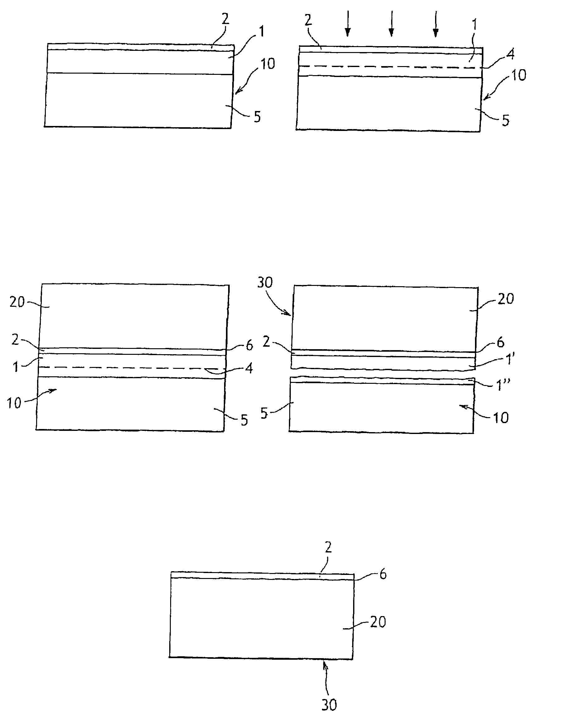
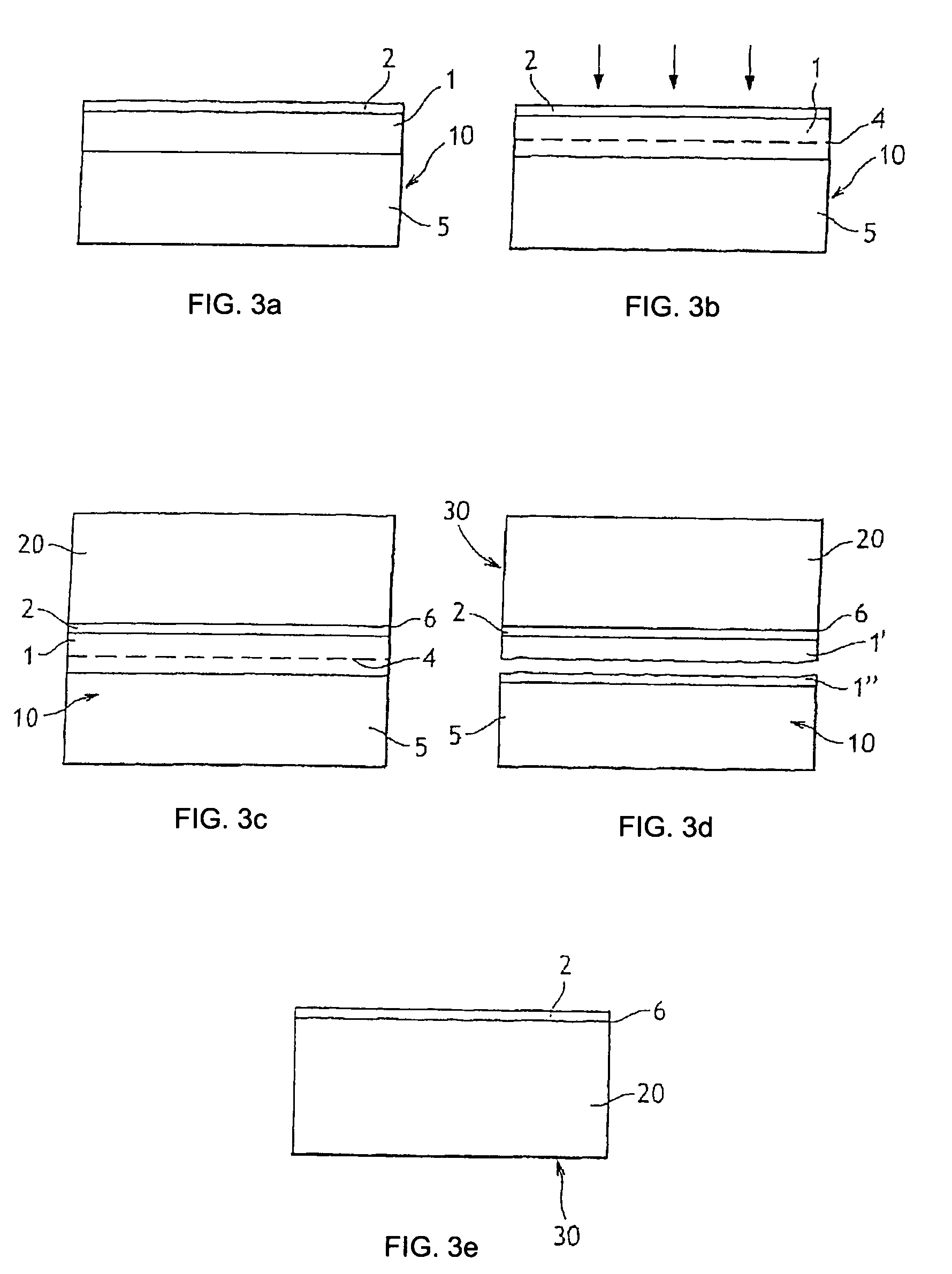
[0023] As noted, the invention relates to a method of forming a structure comprising a layer that is detached from a donor wafer, the donor wafer comprising prior to detachment a first layer made of a semiconductor material comprising germanium. Preferably, the method comprises the following steps: [0024] (a) formation of a weakness zone in the thickness of the layer comprising germanium [0025] (b) bonding the donor wafer to a host wafer; and [0026] (c) supplying energy so as to weaken the donor wafer at the level of the weakness zone. Step (a) is advantageously carried out by subjecting the donor wafer to co-implantation of at least two different atomic species, while step (c) is advantageously carried out by performing a thermal treatment at a temperature between 300° C. and 400° C., for a duration that can last up from 30 minutes to four hours.

[0027] Other potential characteristics of the method according to the invention are as follows:

[0028] The thermal treatment of step (c) ...


PUM


Abstract

A method for forming a structure that includes a layer that is removed from a donor wafer that has a first layer made of a semiconductor material containing germanium. The method includes the steps of forming a weakness zone in the thickness of the first layer; bonding the donor wafer to a host wafer; and supplying energy so as to weaken the donor wafer at the level of the zone of weakness. The zone of weakness is formed by subjecting the donor wafer to a co-implantation of at least two different atomic species, while the bonding is carried out by performing a thermal treatment at a temperature between 300° C. and 400° C. for a duration of from 30 minutes to four hours.

Description

CROSS-REFERENCE TO RELATED APPLICATIONS [0001] This application is a continuation of International application PCT / FR2005 / 000541 filed Mar. 7, 2005 and a continuation-in-part of application Ser. Nos. 11 / 058,992 and 11 / 059,122, each filed Feb. 16, 2005. The entire content of each prior application is expressly incorporated herein by reference thereto.FIELD OF THE INVENTION [0002] The invention relates to a method of forming a structure comprising a layer taken off or transferred from a donor wafer, where the donor wafer comprises, before taking off or transferring, a first layer made of a semi-conductor material comprising germanium. The method generally comprises the successive steps of forming a weakness zone in the thickness of said first layer comprising germanium; bonding the donor wafer to a host wafer; supplying energy so as to weaken the donor wafer at the level of the weakness zone. This energy supply may lead to disunite or detach the layer from the donor wafer at the level...

Claims


Application Information

Patent Timeline
Patent Type & Authority Applications(United States)
IPC IPC(8): H01L21/30H01L21/46
CPCH01L21/76254
Inventor DAVAL, NICOLASAKATSU, TAKESHINGUYEN, NGUYET-PHUONGRAYSSAC, OLIVIERBOURDELLE, KONSTANTIN
Owner S O I TEC SILICON ON INSULATOR THECHNOLOGIES
Why Eureka
Try Eureka