Method for correcting crosstalk

a crosstalk and crosstalk technology, applied in the field of crosstalk correction, can solve the problems of delay variation, function error that logic is inverted, timing limitation infringement, etc., and achieve the effect of not increasing area and power consumption

Inactive Publication Date: 2006-01-19
SOCIONEXT INC
View PDF3 Cites 30 Cited by
  • Summary
  • Abstract
  • Description
  • Claims
  • Application Information

AI Technical Summary

Benefits of technology

[0010] Accordingly, the main object of the present invention is to provide a method for correcting crosstalk, in which the timing limitation infringement and function error due to crosstalk can be corrected without increasing the area and power consumption.

Problems solved by technology

In recent years, with the miniaturization in semiconductor manufacturing technology, crosstalk cannot be ignored.
This phenomenon causes delay variation, timing limitation infringement, or the function error that logic is inverted.
However, the above-mentioned conventional methods for preventing crosstalk have problems that layout resources are consumed for the insertion of buffers or shield wiring, or the upgrade of the cell, that the area is increased, or that an increase in the capacitance and the use of a cell with large current driving capability lead to increased power consumption.
Furthermore, as for the wiring detour, new coupling capacitance with another wiring is generated in the detour to thereby cause new crosstalk, which deteriorates the convergence of timing design.

Method used


Image

  • Method for correcting crosstalk
  • Method for correcting crosstalk
  • Method for correcting crosstalk

Examples


embodiment 1

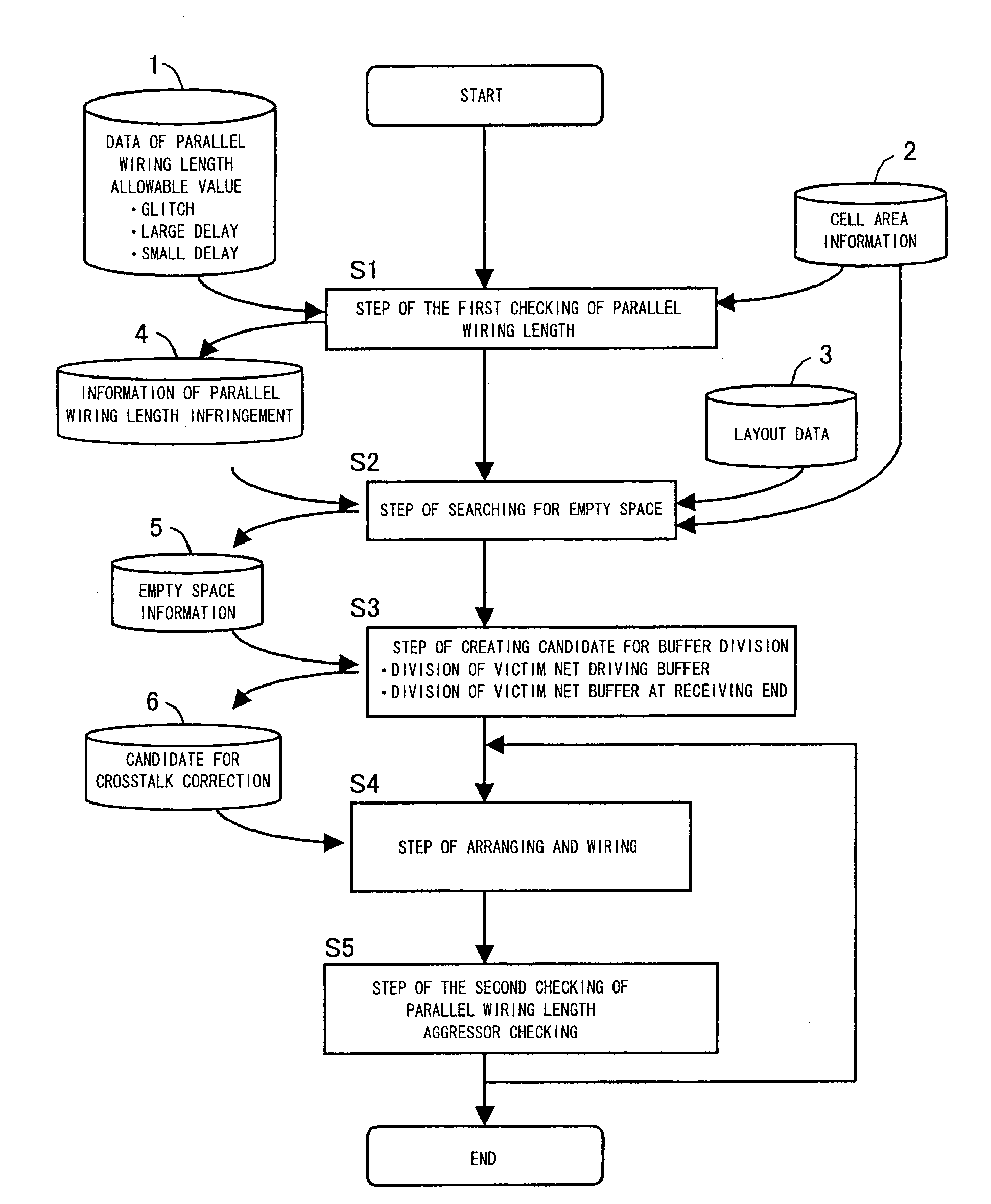
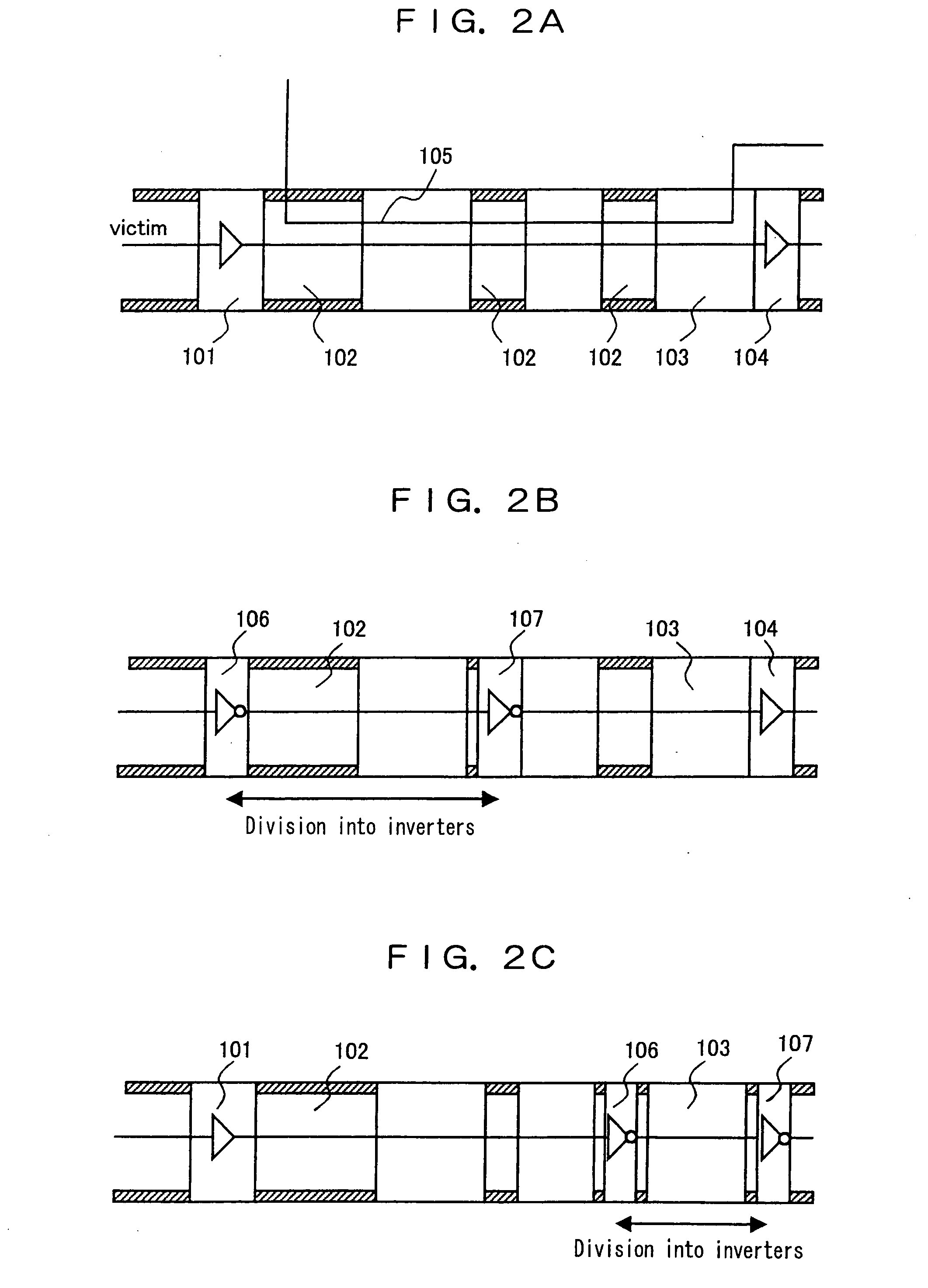
[0083]FIG. 1 is a flow diagram showing a method for correcting crosstalk (buffer division) according to a first embodiment of the present invention, and FIGS. 2A, 2B and 2C are diagrams showing specific examples thereof.

[0084] In FIG. 1, S1 designates the step of the first checking of a parallel wiring length; S2, the step of searching for an empty space on a wiring route; S3, the step of creating a candidate for buffer division; S4, the step of arranging and wiring; and S5, the step of the second checking of the parallel wiring length. A reference numeral 1 designates data of a parallel wiring length allowable value; a reference numeral 2, layout data; a reference numeral 3, cell area information; a reference numeral 4, information of parallel wiring length infringement; a reference numeral 5, empty space information; and a reference numeral 6, a candidate for crosstalk correction.

[0085] In FIGS. 2A, 2B and 2C, a reference numeral 101 designates a driving cell of a victim net; a ...

embodiment 2

[0097]FIG. 3 is a flow diagram showing a method for correcting crosstalk according to a second embodiment of the present invention and FIGS. 4A, 4B and 4C are diagrams showing specific examples thereof.

[0098] In FIG. 3, S1, S2, S4 and S5 designate the same steps as those in FIG. 1 according to the first embodiment. S3a designates the step of creating a candidate for cell movement. Reference numerals 1 to 6 also designate the same components as those in FIG. 1 according to the first embodiment. In FIGS. 4A, 4B and 4C, reference numerals 101 to 105 designate the same components as those in FIGS. 2A, 2B and 2C according to the first embodiment.

[0099] With respect to the method for correcting crosstalk having the above-mentioned configuration according to the present embodiment, behaviors thereof are described below.

[0100] Referring to FIG. 3, in step S1 of the checking of a parallel wiring length, the input data 1 of a parallel wiring length allowable value is referred to and the in...

embodiment 3

[0110]FIG. 5 is a flow diagram showing a method for correcting crosstalk (victim net logic resynthesis) according to a third embodiment of the present invention and FIGS. 6A and 6B are diagrams showing specific examples thereof.

[0111] In FIG. 5, S1, S2, S4 and S5 designate the same steps as those in FIG. 1 according to the first embodiment. S3b designates the step of victim net logic synthesis. Reference numerals 1 to 6 also designate the same components as those in FIG. 1 according to the first embodiment. A reference numeral 7 designates logic connection information.

[0112] Referring to FIGS. 6A and 6B, a reference numeral 111 designates a driving cell AND gate of a victim net #1; a reference numeral 112, victim net #1 wiring; a reference numeral 113, a victim net #2 driving cell; a reference numeral 114, fan-out ¥1 wiring of the victim net #2; a reference numeral 115, fan-out ¥2 wiring of the victim net #2; a reference numeral 116, a fan-out ¥1 driving cell at the next stage; a ...


PUM


Abstract

In a semiconductor integrated circuit, there is provided a method for correcting crosstalk, which exerts an influence via coupling capacitance between wiring by the signal transitions between adjacent wiring, comprising the step of creating a candidate for buffer division, the step of creating a candidate for cell movement, or the step of victim net logic synthesis. Thereby, the crosstalk is corrected through the buffer division, the cell movement, or an increase of elements in number by logic decomposition, logic inversion and a change of fan-outs in number.

Description

BACKGROUND OF THE INVENTION [0001] The present invention relates to a method for correcting crosstalk as one of layout corrections to render crosstalk between wires harmless in layout designing of a semiconductor integrated circuit. [0002] In recent years, with the miniaturization in semiconductor manufacturing technology, crosstalk cannot be ignored. Crosstalk exerts an influence via coupling capacitance between adjacent wires by the transition of signals thereof in a semiconductor integrated circuit. This phenomenon causes delay variation, timing limitation infringement, or the function error that logic is inverted. [0003] Accordingly, in the layout design of a semiconductor integrated circuit, there has been needed crosstalk correction for correcting the layout in order not to cause the timing limitation infringement or logic inversion due to crosstalk as well as the detection of the occurrence of crosstalk. [0004] In a conventional method for correcting crosstalk, a repeater buf...

Claims


Application Information

Patent Timeline
Patent Type & Authority Applications(United States)
IPC IPC(8): G06F17/50H01L21/66H01L21/82H01L21/822H01L27/04
CPCG06F17/5045G06F17/5036G06F30/367G06F30/30
Inventor AMEKAWA, NAOKI
Owner SOCIONEXT INC
Why Eureka
Try Eureka