
Semiconductor device

a technology of semiconductor devices and shielding devices, which is applied in the direction of semiconductor devices, semiconductor/solid-state device details, electrical apparatus, etc., can solve the problems of increasing the current consumption at standby during the entire operation of the integrated circuit, the current of the off transistor is much more serious, and the protection function cannot be sufficiently implemented, so as to prevent the generation of esd, and maintain the leakage current small

Inactive Publication Date: 2014-12-09
ABLIC INC
View PDF28 Cites 0 Cited by
  • Summary
  • Abstract
  • Description
  • Claims
  • Application Information

AI Technical Summary

Benefits of technology

[0015]Through the means as described above, there can be obtained a semiconductor device including an NMOS transistor for ESD protection provided with a sufficient ESD protection function while keeping the off leak current small by preventing the generation of the leak current characteristic to the shallow trench isolation structure or by avoiding a region which generates leak current, without increasing manufacturing steps or an occupation area thereof.

Problems solved by technology

The width W of the off transistor is large as described above, and thus an off leak current at standby during operation becomes larger, which leads to a problem of increase in the current consumption at standby during operation of the entire integrated circuit (IC) carrying the off transistor.
In particular, in the case of a semiconductor device in which a shallow trench is used for device isolation, there is a problem in that an area adjacent to the shallow trench includes a region such as a crystal defect layer or the like which easily generates leak current, arising from the structure itself or a manufacturing method thereof.
Further, off leak current of the off transistor poses much more serious problems.
However, when the width W is made small to reduce the off leak current of the off transistor, protection function cannot be sufficiently implemented.
Besides, in the semiconductor device in which a plurality of transistors are provided to cut the current path between the power line (Vdd) and the ground (Vss) as proposed in JP 2002-231886 A, an occupation area thereof increases because the semiconductor device includes the plurality of transistors, leading to an increase in cost of the semiconductor device.

Method used


Image

  • Semiconductor device
  • Semiconductor device
  • Semiconductor device

Examples


first embodiment

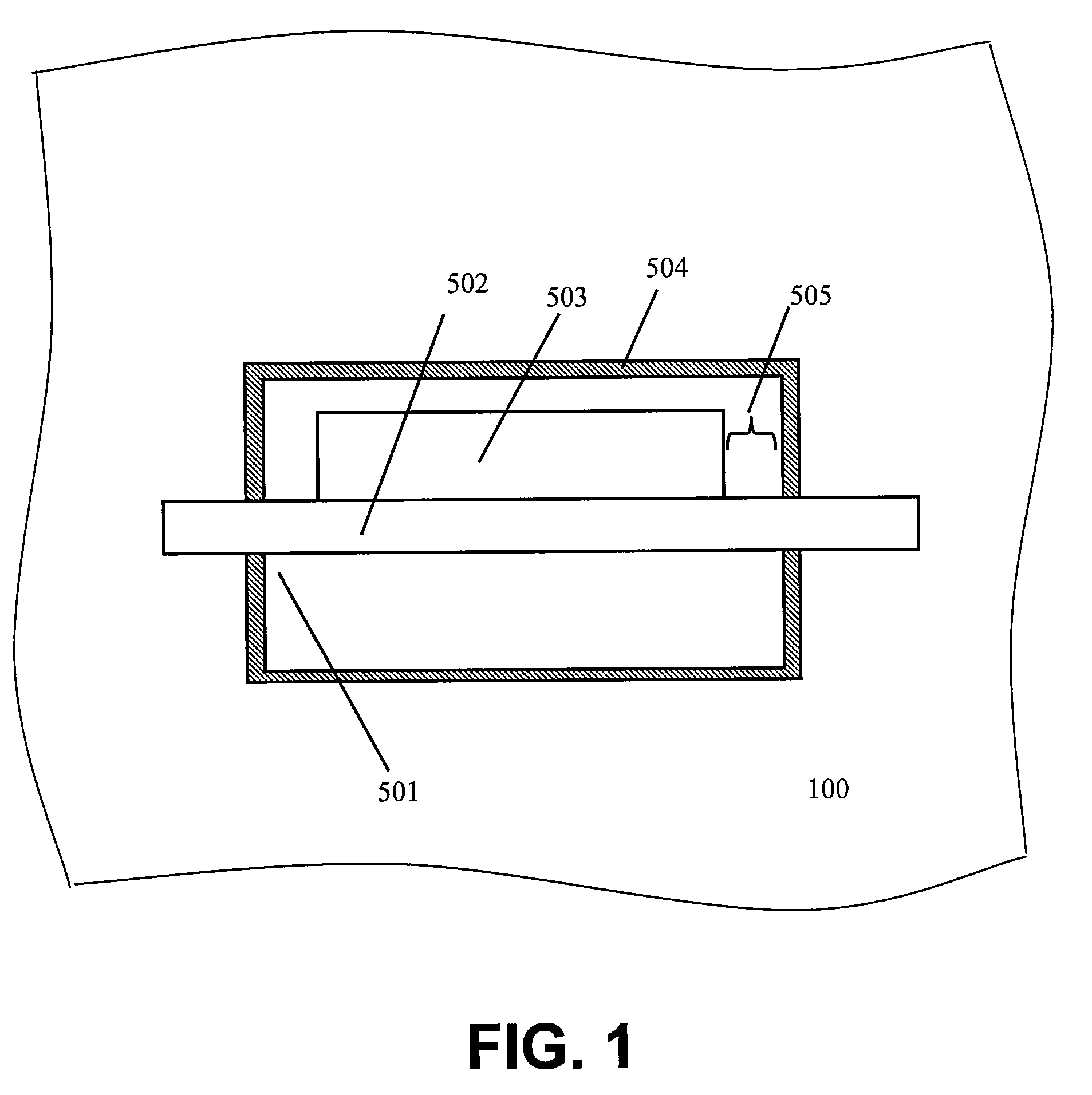
[0019]FIG. 1 is a schematic plan view showing an NMOS transistor for ESD protection of a semiconductor device according to a first embodiment of the present invention.

[0020]A pair of a source region 501 and a drain region 503 which are formed of an n-type heavily-doped impurity region are arranged on a p-type semiconductor substrate 100, a gate insulating film (not shown) made of a silicon oxide film or the like is placed between the source region 501 and the drain region 503, and a gate electrode 502 made of a polysilicon or the like is formed on an upper surface of the gate insulating film. A shallow trench structure is used for insulation from other elements, and a perimeter of the transistor is surrounded by a shallow trench isolation region 504. In this case, the drain region 503 is placed apart from the shallow trench isolation region 504, and a separation region 505 is formed between the drain region 503 and the shallow trench isolation region 504.

[0021]A region adjacent to t...

second embodiment

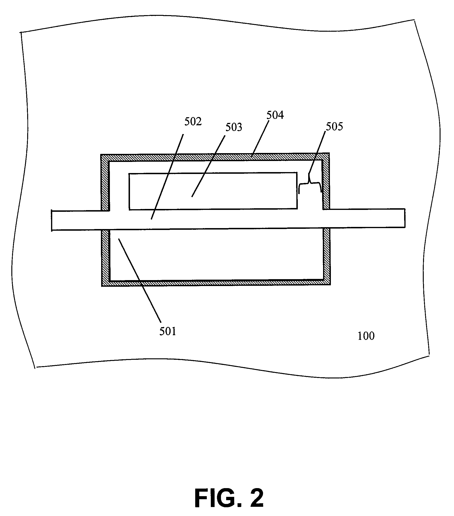
[0027]FIG. 2 is a schematic plan view showing an NMOS transistor for ESD protection of a semiconductor device according to a second embodiment of the present invention. The second embodiment is different from the first embodiment shown in FIG. 1 in that the separation region 505 placed between the drain region 503 and the shallow trench isolation region 504 is formed in a self-alignment manner in a region where the gate electrode 502 is extended.

[0028]In a generally-employed semiconductor manufacturing step, the gate electrode 502 is formed, and then the drain region 503 and the source region 501 are formed in a self-alignment manner with the gate electrode 502 using an ion implantation method or other methods in many cases. In the second embodiment shown in FIG. 2, in forming the drain region 503, the separation region 505 is automatically formed in the region where the gate electrode 502 is extended, with the result that the manufacturing step can be more simplified. Other parts a...

third embodiment

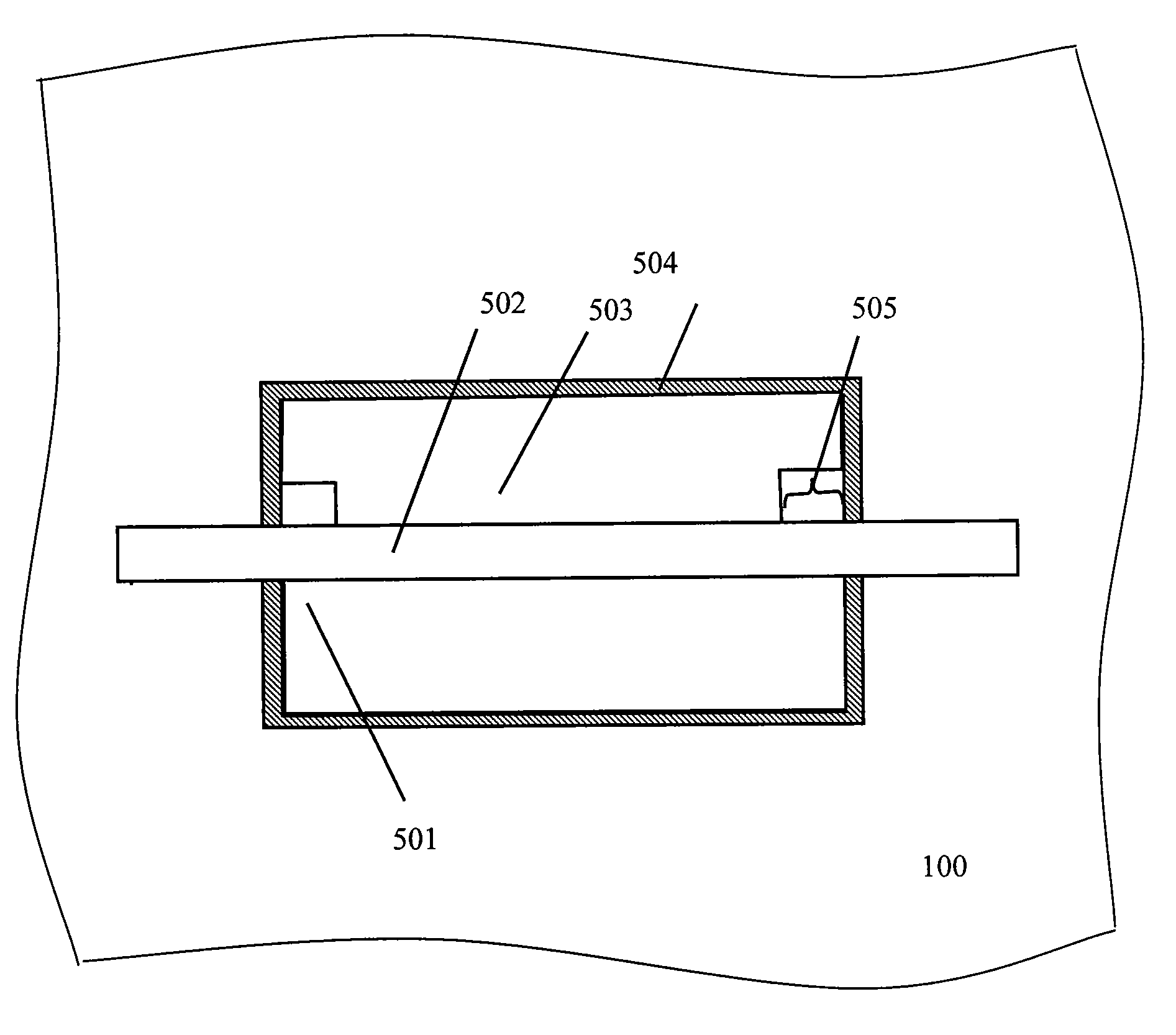
[0029]FIG. 3 is a schematic plan view showing an NMOS transistor for ESD protection of a semiconductor device according to a third embodiment of the present invention. The third embodiment is different from the first embodiment shown in FIG. 1 in that only regions of the drain region 503, which are adjacent to the gate electrode 502, are placed apart from the shallow trench isolation region 504.

[0030]A region of the NMOS transistor for ESD protection having the shallow trench isolation structure, where a largest amount of off leak current flows, is a channel region being adjacent to the shallow trench isolation region 504 and existing under the gate electrode 502. A junction between the drain region 503 in the vicinity of the shallow trench isolation region 504 and the p-type substrate 100 or a well region (not shown) is another part where the leak current is generated, but the leak current generated in the junction does not pose a serious problem in many cases.

[0031]The third embod...


PUM


Abstract

In order to suppress an off leak current of an off transistor for ESD protection, in an NMOS for ESD protection whose isolation region has a shallow trench structure, a drain region is placed apart from the shallow trench isolation region so as not to be in direct contact with the shallow trench isolation region in a region where the drain region of the NMOS transistor for ESD protection is adjacent to at least a gate electrode of the NMOS transistor for ESD protection.

Description

RELATED APPLICATIONS[0001]This application claims priority under 35 U.S.C. §119 to Japanese Patent Application No. JP2007-215947 filed on Aug. 22, 2007, the entire content of which is hereby incorporated by reference.BACKGROUND OF THE INVENTION[0002]1. Field of the Invention[0003]The present invention relates to a semiconductor device having metal oxide semiconductor (MOS) transistors isolated by shallow trench structure, and using an n-type MOS (NMOS) transistor as an electrostatic discharge (hereinafter, referred to as ESD) protection element.[0004]2. Description of the Related Art[0005]In a semiconductor device having MOS transistors, an off transistor, which is an NMOS transistor provided in an off-state whose gate potential is fixed to a ground (Vss), is used as an ESD protection element for preventing breakdown of an internal circuit due to static electricity supplied from a pad provided for external connection.[0006]Since the off transistor must flow a large amount of current...

Claims


Application Information

Patent Timeline
Patent Type & Authority Patents(United States)
IPC IPC(8): H01L29/66H01L29/78H01L27/02H01L21/70
CPCH01L27/0266H01L29/78
Inventor TAKASU, HIROAKI
Owner ABLIC INC
Learn More