Resonator

a resonance and frequency technology, applied in the field of radiofrequency circuits, can solve the problems of increasing manufacturing costs and space occupancy in micro wave bands, and achieve the effects of reducing the resonance frequency in the resonator structure, reducing the effect of such a resonance frequency, and considerable downsizing

Active Publication Date: 2006-01-26
PANASONIC CORP
View PDF3 Cites 7 Cited by
  • Summary
  • Abstract
  • Description
  • Claims
  • Application Information

AI Technical Summary

Benefits of technology

[0053] According to the first aspect of the present invention, the first ground conductor layer having the first slot formed into a spiral shape and the second ground conductor layer having the second slot formed also into a spiral shape are disposed on the surface and the back surface of the dielectric substrate, and the first slot and the second slot are disposed so as to overlap as viewed from the top face (i.e., disposed such that there is an overlapped portion in the thickness direction of the dielectric substrate with respective formation positions being different), so that under the conditions that a radio-frequency displacement current flows in the same direction in the respective slots, a so-called even mode can be induced in the overlapped portion of the respective slots, thereby allowing an apparent dielectric constant to be increased. As a result, it becomes possible to decrease the resonance frequency in the resonator structure having the layout structure of the respective slots in the laminated state to be lower than the resonance frequency in the resonator structure in which each slot exists independently. More particularly, it becomes possible to provide a resonator which can produce a resonance phenomenon at a resonance frequency lower than the resonance frequency of the first slot and the resonance frequency of the second slot.
[0054] Further, the reduction effect of such a resonance frequency can be increased as the overlapped portion of the respective slots is increased. Thus, the reduction effect of the resonance frequency can be obtained, and this makes it possible to achieve the resonance phenomenon of a half-wave resonance mode with the space occupancy of the conventional one resonator, the half-wave resonance mode having a resonator length longer than the resonator length in the conventional resonator structure having the structure in which, for example, the respective slots adjacently disposed on the same plane are coupled in series, thereby allowing considerable downsizing, area reduction and volume saving of the resonator.
[0055] According to another aspect of the present invention, such a reduction effect of the resonance frequency can be enhanced by disposing the slots so that the spiral winding direction of the first slot and the spiral winding direction of the second slot are opposite to each other.
[0056] Moreover, the reduction effect of the resonance frequency can be further enhanced by disposing the slots so that the centers and outer edges of the spirals of the respective slots are aligned with each other in the laminating direction.
[0057] Further, by disposing the respective slots so that the outer termination portion of the first slot and an outer termination portion of the second slot are disposed at positions symmetric with respect to a center point of the spiral of the slot, the resonator length can be increased and the reduction effect of the resonance frequency can be further enhanced.
[0058] Moreover, by further providing the connection through conductor disposed through the dielectric substrate for connecting a ground conductor region outside an outer edge of the first slot and a ground conductor region outside the second slot, the radio-frequency ground state of the respective ground conductor layers can be strengthened. Thus, even if difference in the connection state (mounting state) when the resonator is connected to an external circuit causes difference in the ground state between the first ground conductor layer and the second ground conductor layer, strengthening the ground state allows the potentials of the ground conductor layers to be identical, thereby enabling the characteristics of the resonator to be stabilized.

Problems solved by technology

However, since further downsizing of such resonators are demanded, the slot circuit which produces resonance at a size that is equivalent to the size of ½ wavelength of an electromagnetic wave suffers such a problem that space occupancy increases in micro wave bands.
Moreover, since shortening of an effective wavelength in the circuit substrate is also effective for decreasing the resonance frequency, use of high dielectric constant materials is possible, while at the same time, it requires special manufacturing process unlike substrates made of resin materials or general semiconductor substrates, and causes increase in manufacturing costs.

Method used


Image

  • Resonator
  • Resonator
  • Resonator

Examples


first embodiment

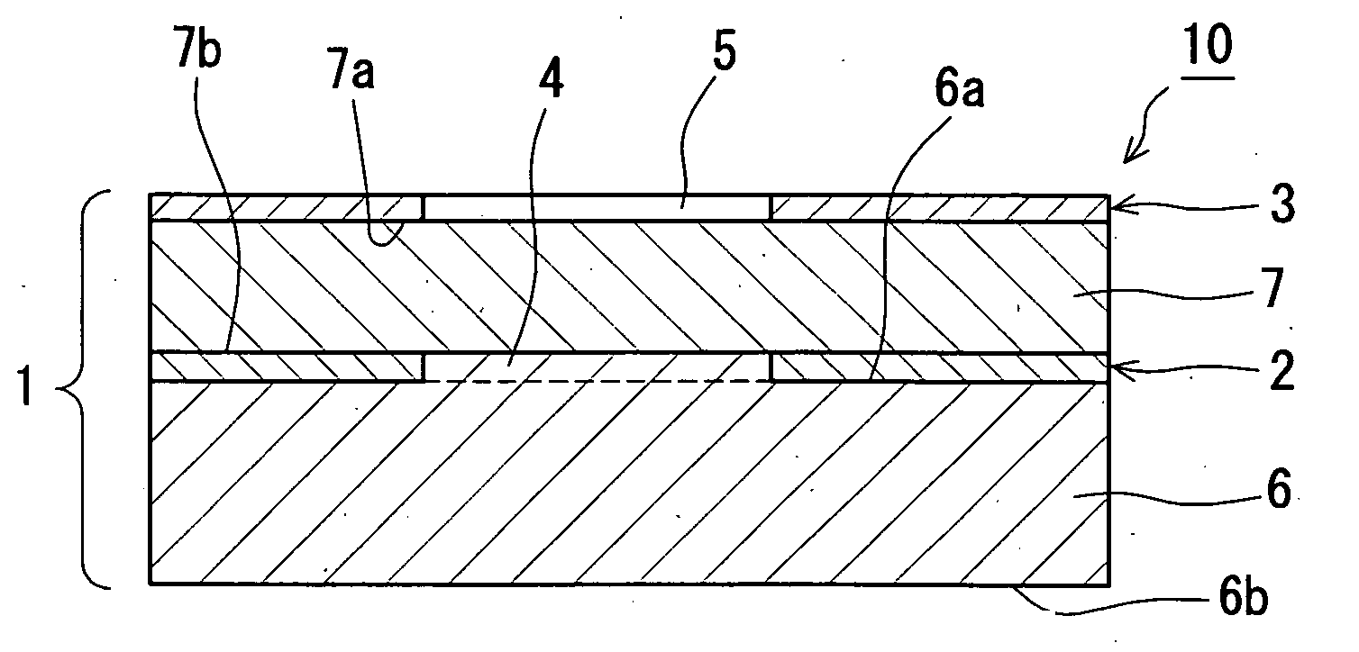
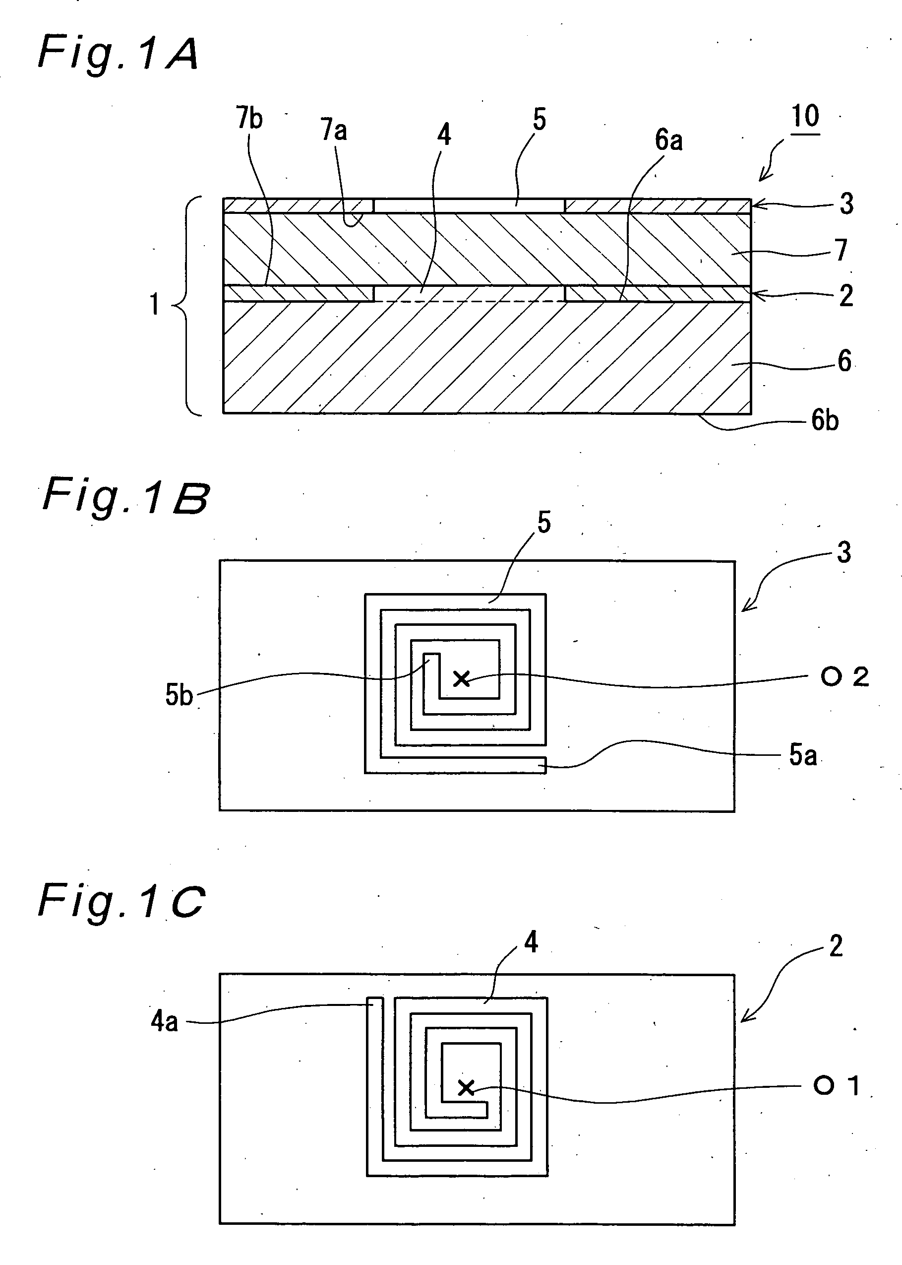
[0103]FIG. 1A is a cross sectional view showing a resonator 10 using a radio-frequency circuit according to the first embodiment of the present invention.

[0104] In FIG. 1, the resonator 10 has a multilayer dielectric substrate 1 having a laminated structure comprises a first dielectric substrate 6 and a second dielectric substrate 7. Moreover, the respective dielectric substrates 6 and 7 are laminated so that a front surface 6a (top face in the drawing) of the first dielectric substrate 6 and a back surface 7b (bottom face in the drawing) of the second dielectric substrate 7 are bonded to each other, and in this bonding portion, a first ground conductor layer 2 is formed. Moreover, a second ground conductor layer 3 is formed on a front surface 7a (top face in the drawing) of the second dielectric substrate 7, i.e., the front surface of the multilayer dielectric substrate 1. It is to be noted that the front surface 6a of the first dielectric substrate 6 and the front surface 7a of t...

working example 1

[0133] Next, working examples 1-1 to 1-7 of the resonator in the first embodiment will be described. For the purpose of comparing the structure and the resonance frequency of working examples with those of comparative examples, the working examples 1-1 are shown in Table 1 while the working examples 1-7 are shown in Table 2.

TABLE 1AdditionalresinSpiralConnection ofsubstratewindinggroundResonancethicknessdirection ofOverlap ofconductorfrequencyFirst slotSecond slot(μm)two slotstwo slotslayer(GHz)Working examplePresentPresent130Opposite——1.881-1Working examplePresentPresent 80Opposite——1.481-2Working examplePresentPresent 30Opposite——0.811-3Working examplePresentPresent130IdenticalOverlapped—3.131-4Working examplePresentPresent130IdenticalNot—2.691-5overlapped(180-degreerotation)Working examplePresentPresent130Opposite—Connected in1.911-6vicinity ofslotComparativePresentAbsent130———4.10example 1-1ComparativeAbsentPresent130———5.07example 1-2ComparativePresentPresent130Opposite—Conne...

second embodiment

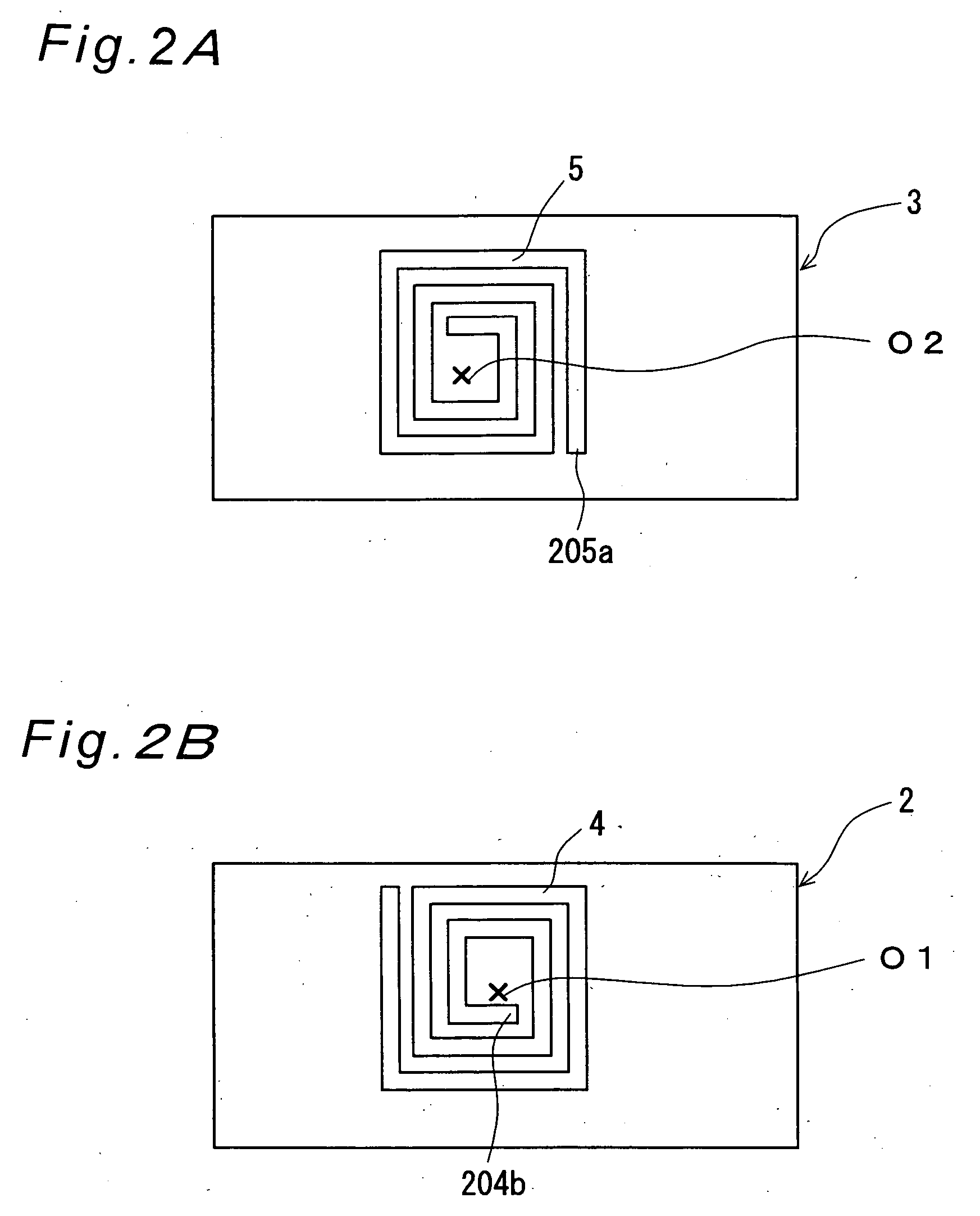
[0148] It is to be understood that the present invention is not limited to the above embodiment and can be embodied in other various aspects. For example, the cross sectional view showing a structure of a resonator 20 according to the second embodiment of the present invention is shown in FIG. 5A. It is to be noted that in FIG. 5A, component parts same as in FIG. 1A, FIG. 1B and FIG. 1C are designated by the same reference numerals and the description thereof is omitted.

[0149] As shown in FIG. 5A. a multilayer dielectric substrate 21 is structured from a laminated structure composed of a first dielectric substrate 6 and a second dielectric substrate 7. In a bonding portion between a front surface 6a of the first dielectric substrate 6 and a back surface 7b of the second dielectric substrate 7, a ground conductor layer 2 (that is equivalent to the first ground conductor layer 2 in the first embodiment) is formed. Moreover, a conductor interconnection layer 23 is formed on the front ...


PUM


Abstract

Inside a multilayer dielectric substrate (1), there are a spiral-shaped first slot (4) set in a part of a first ground conductor layer (2) and a spiral-shaped second slot (5) in a part of a second ground conductor layer (3) put on the front surface of the multilayer dielectric substrate, the first slot and the second slot are opposite in a spiral winding direction and the first slot and the second slot overlap with each other as viewed from the top face, so that a resonance phenomenon can be produced at a frequency lower than a resonance frequency of a resonator with a conventional structure.

Description

BACKGROUND OF THE INVENTION [0001] The present invention relates to a radio-frequency circuit for transmitting or radiating radio-frequency signals in frequency bands such as a microwave band and a milliwave band, and more particularly to a resonator for producing a resonance phenomenon at a specified design frequency (resonance frequency) in these bands. [0002] In recent years, radio communication equipment with smaller size and higher functionality has been developed, which has allowed explosive growth of radio communication equipment typified by cell-phones and the like. In the future, it is predicted that there will be continuous demands for further downsizing of the radio communication equipment or each device for use in the radio communication equipment without damage on the functionality or the low cost thereof. [0003] One of resonance circuit elements (resonators) for use in the radio-frequency circuit mounted on the radio equipment includes a radio-frequency circuit element...

Claims


Application Information

Patent Timeline
Patent Type & Authority Applications(United States)
IPC IPC(8): H01P7/08
CPCH01P7/082
Inventor KANNO, HIROSHISAKIYAMA, KAZUYUKISANGAWA, USHIOFUJISHIMA, TOMOYASU
Owner PANASONIC CORP
Why Eureka
Try Eureka