

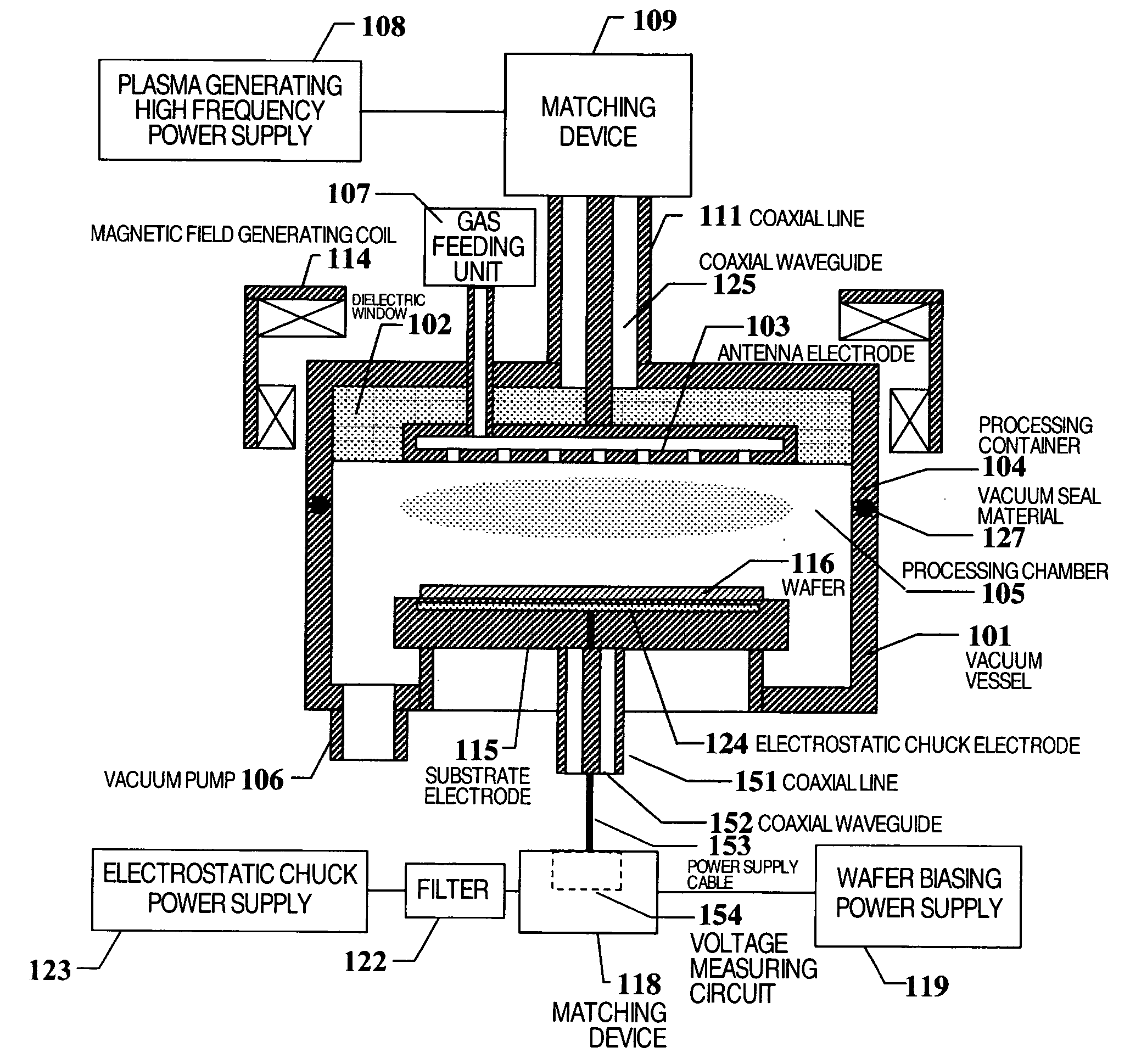
Plasma processing apparatus with resonance countermeasure function
a technology of resonance countermeasure and processing apparatus, which is applied in the direction of mechanical apparatus, threaded fasteners, screwdrivers, etc., can solve the problems of not being able to predict the phenomenon due to the plasma, the influence of the technique on the resonance phenomena, and the accuracy of this technique is significantly reduced, so as to reduce the resonant frequency, reduce the manufacturing cost, and increase the electrostatic capacitance of the heath
- Summary
- Abstract
- Description
- Claims
- Application Information
AI Technical Summary
Benefits of technology
Problems solved by technology
Method used
Image

Examples
Embodiment Construction
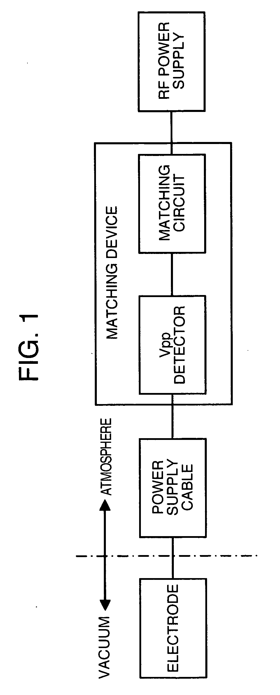
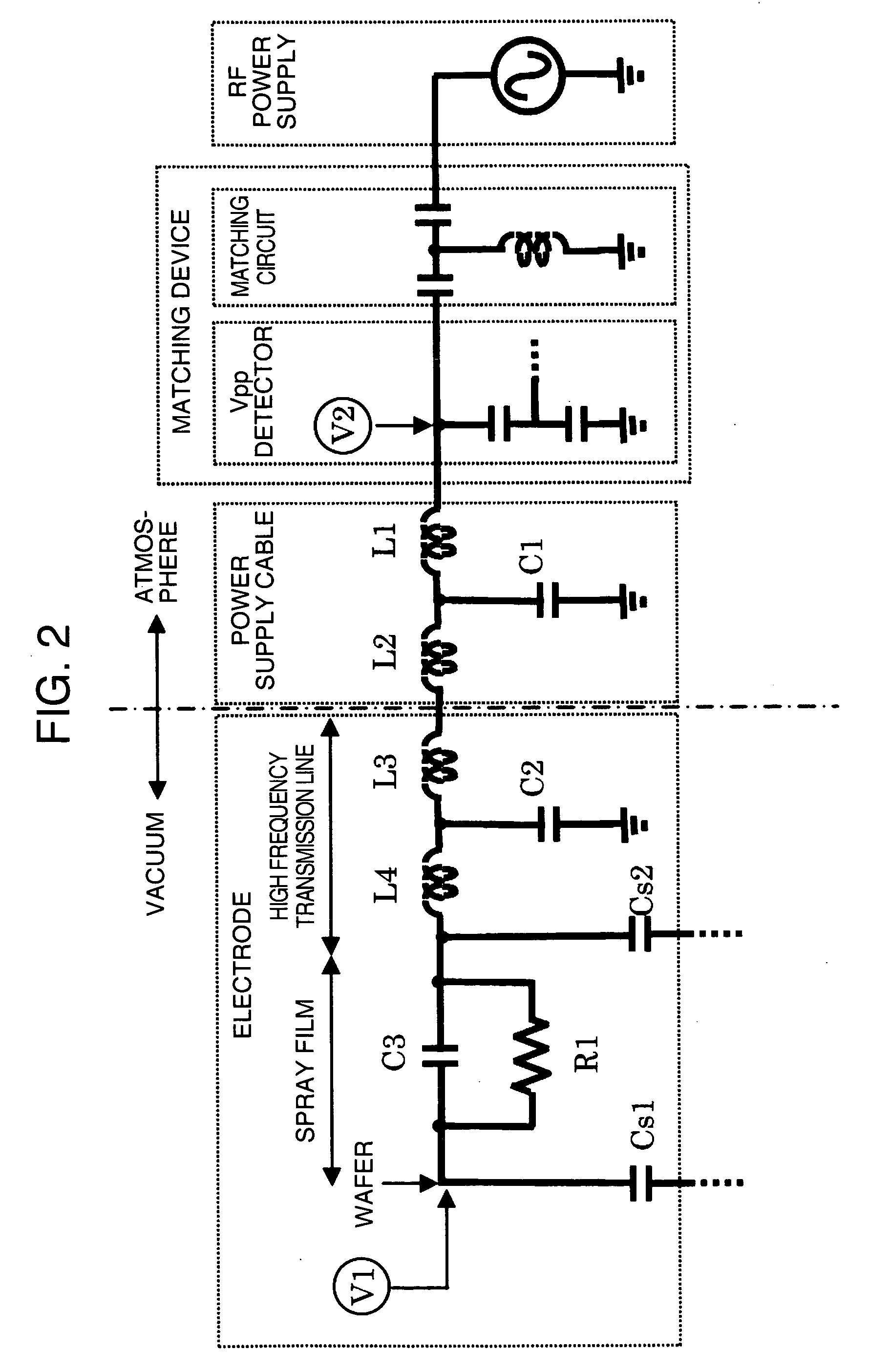
[0065] The resonance cannot be eliminated and it cannot be corrected by computation or calibration as described above. Thus, only the method to solve this problem is to construct the apparatus so that the voltage or phase information at the measurement point can be made equivalent to or equal to that at the electrode (the electrode such as the wafer that makes capacitive coupling with the plasma) to be measured. This apparatus structure needs to raise the resonant frequency not to affect the voltage detection.
[0066] First, the resonant frequency is made as high as possible. Here, the term “the lowest resonant frequency” is represented by a symbol fL. The lowest resonant frequency is defined as the lowest resonant frequency appearing in certain plasma processing apparatus and under a range of the working conditions of this apparatus. Now, the resonant frequency of 4 MHz shown in FIG. 3A is selected and used to indicate the ratio of frequency / 4 MHz on the abscissa as shown in FIG. 3B...
PUM
| Property | Measurement | Unit |
|---|---|---|
| impedance | aaaaa | aaaaa |
| frequencies | aaaaa | aaaaa |
| total stray capacitance Ct | aaaaa | aaaaa |
Abstract
Description
Claims
Application Information