Image sensor with improved charge transfer efficiency and method for fabricating the same

Active Publication Date: 2006-02-02
INTELLECTUAL VENTURES II
View PDF1 Cites 6 Cited by
  • Summary
  • Abstract
  • Description
  • Claims
  • Application Information

AI Technical Summary

Benefits of technology

[0021] It is, therefore, an object of the present invention to provide an image sen

Problems solved by technology

The decreased driving voltage may become one cause of degraded quality of an image in low brightness.
This potential barrier impedes the charge transfer, thereby decreasing the charge transfer effi

Method used


Image

  • Image sensor with improved charge transfer efficiency and method for fabricating the same
  • Image sensor with improved charge transfer efficiency and method for fabricating the same
  • Image sensor with improved charge transfer efficiency and method for fabricating the same

Examples


first embodiment

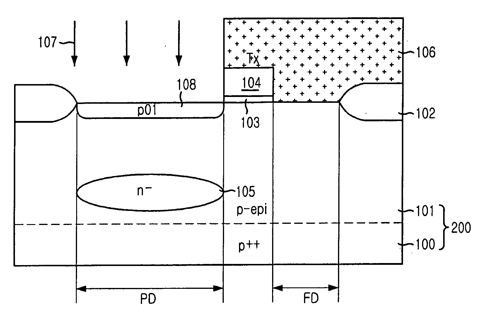
[0041]FIG. 6 is a cross-sectional view showing a part of a unit pixel of an image sensor in accordance with the present invention.

[0042] As shown, the image sensor includes: a gate structure, more specifically, a transfer gate Tx, formed on a p-type semiconductor layer 200; a first p-type impurity (p01) region 108; a pair of first spacers 109 formed on sidewalls of the transfer gate Tx; a second p-type impurity (p02) region 113; a pair of second spacers 114 formed on sidewalls of the first spacers 109; a third p-type impurity (p03) region 117; and an n−-type impurity region 105 for use in a photodiode.

[0043] The p-type semiconductor layer 200 includes a highly doped p++-type substrate 100 and a p-epi layer 101. The gate structure includes a gate insulation layer 103 and a conductive layer 104.

[0044] The first p-type impurity (p01) region 108 extends to a first depth from a surface of the semiconductor layer 200 as being aligned with one side of the transfer gate Tx. The second p-t...

second embodiment

[0047]FIG. 7 is a cross-sectional view showing a part of a unit pixel of an image sensor in accordance with the present invention. Herein, it should be noted that the same reference numerals are used for the same configuration elements described in FIG. 6 and thus, detailed description of such configuration elements will be omitted.

[0048] As shown in FIG. 7, the image sensor includes: a gate structure, more specifically, a transfer gate Tx, formed on a p-type semiconductor layer 200; a highly doped n+-type floating diffusion (FD) region 110; a plurality of device isolation regions 102; a first p-type impurity (p01) region 108; a pair of first spacers 109 formed on sidewalls of the transfer gate Tx; a second p-type impurity (p02) region 113; a screening insulation layer 118; a third p-type impurity (p03) region 117; and an n−-type impurity region 105 for use in a photodiode.

[0049] The first p-type impurity (p01) region 108 extends to a first depth from a surface of the semiconductor...


PUM


Abstract

An image sensor includes: a first impurity region of the first conductive type aligned with one side of the gate structure and extending to a first depth from a surface portion of the semiconductor layer; a first spacer formed on each sidewall of the gate structure; a second impurity region of the first conductive type, aligned with the first spacer and extending to a second depth that is larger than the first depth from the surface portion of the semiconductor layer; a second spacer formed on each sidewall of the first spacer; a third impurity region of the first conductive type aligned with the second spacer and extending to a third depth that is larger than the second depth from the surface portion of the semiconductor layer; and a fourth impurity region of a second conductive type beneath the third impurity region.

Description

FIELD OF THE INVENTION [0001] The present invention relates to an image sensor and a method for fabricating the same; and, more particularly, to an image sensor with improved charge transfer efficiency and a method for fabricating the same. DESCRIPTION OF RELATED ARTS [0002] Image sensors are semiconductor devices that convert an optical image into an electrical signal. Examples of such image sensors are charge coupled devices (CCDs) and complementary metal-oxide-semiconductor (CMOS) image sensors. [0003] CCDs are devices where charge carriers transferred from metal-oxide-semiconductor (MOS) capacitors are stored into the MOS capacitors closely allocated around the CCDs. On the other hand, CMOS image sensors take a switching mode that sequentially detects outputs by using MOS transistors fabricated in the same number of pixels via CMOS technology using a control circuit and a signal processing circuit as a peripheral circuit. Particularly, CMOS image sensors have been widely used in...

Claims


Application Information

Patent Timeline
IPC IPC(8): H01L21/00H01L33/00H01L27/146H01L31/10H04N5/374H04N5/3745
CPCH01L27/1463H01L27/14632H01L31/035236H01L27/14687H01L27/14689H01L27/14647H01L21/22H01L27/146H01L31/10
Inventor PARK, JAE-YOUNGLIM, YOUN-SUB
Owner INTELLECTUAL VENTURES II
Why Eureka
Try Eureka