Pixel circuit, display device, driving method of pixel circuit, and driving method of display device

a technology of display device and pixel circuit, which is applied in the direction of instruments, static indicating devices, etc., can solve the problems of difficulty in realizing a large and high-definition display, degradation of brightness with the passage of time, etc., and achieve the reduction of the driving capability of the drive transistor, the effect of preventing brightness degradation and reducing the mobility of the drive transistor

Inactive Publication Date: 2006-02-02
SONY CORP
View PDF2 Cites 89 Cited by
  • Summary
  • Abstract
  • Description
  • Claims
  • Application Information

AI Technical Summary

Benefits of technology

[0021] According to another embodiment of the present invention, there is provided a driving method of a pixel circuit disposed at a part where a scanning line and a signal line intersect each other, the pixel circuit including at least an electrooptic element, a drive transistor, a sampling transistor, and a retaining capacitance, the drive transistor having a gate connected to an input node, a source connected to an output node, and a drain connected to a predetermined power supply potential, the electrooptic element having one terminal connected to the output node and another terminal connected to a predetermined potential, the sampling transistor being connected between the input node and the signal line, the retaining capacitance being connected to the input node, the driving method including the steps of: the sampling transistor operating when selected by the scanning line, sampling an input signal from the signal line, and retaining the input signal in the retaining capacitance; the drive transistor supplying a driving current to the electrooptic element according to a signal potential retained in the retaining capacitance; in order to compensate for a decrease in the driving current which decrease is attendant on a secular change of the drive transistor by detecting the decrease in the driving current from a side of the output node and feeding back a result of detection to a side of the input node, accumulating charge carried by the driving current for a certain period of time and obtaining a detection potential corresponding to an amount of charge accumulated; and obtaining a difference by comparing a level of the input signal with a level of the detection potential and adding a potential corresponding to the difference to the signal potential retained in the retaining capacitance.
[0035] A pixel circuit according to an embodiment of the present invention incorporates a compensating circuit to compensate for a decrease in driving current with a secular change of a drive transistor. This compensating circuit detects a decrease in the driving current from a side of an output node and feeds back a result of detection to a side of an input node, whereby the decrease in the driving current is cancelled by circuit means. Therefore, even when the mobility of the drive transistor is decreased and thereby the driving capability of the drive transistor is decreased, feedback to the side of the input node is performed so as to compensate for the decrease. Consequently, the driving current can be maintained at the same constant level as an initial level for a long period of time. It is thereby possible to prevent degradation in brightness which degradation is caused by the drive transistor, and thus maintain screen uniformity over a long period of time.
[0036] A pixel circuit according to another embodiment of the present invention incorporates a compensating circuit to compensate for a decrease in brightness due to a secular change of a light emitting element by circuit means in a pixel unit. In addition, it is possible to compensate for initial variations in brightness of light emitting elements which variations appear in pixels. This compensating circuit uses as a principle the fact that a voltage drop occurring in a light emitting element increases according to a secular change of the light emitting element. That is, when brightness is gradually decreased due to degradation of the light emitting element with the passage of time, the voltage drop tends to be conversely increased according to the decrease. This increasing voltage drop is detected from the side of an output node, and a signal potential corresponding to the detected voltage drop is fed back to the side of an input node. The drive transistor always supplies a driving current from the output node in a direction to compensate for decrease in brightness of the light emitting element according to the fed-back signal potential. It is thereby possible to prevent degradation in brightness of the light emitting element, and thus maintain screen uniformity over a long period of time. In addition, it is possible to compensate for initial variations in brightness of light emitting elements which variations appear in pixels, and thereby improve screen uniformity.

Problems solved by technology

The former system offers a simple structure, but presents for example a problem of difficulty in realization of a large and high-definition display.
However, there is a problem in that degradation in brightness occurs with the passage of time.

Method used


Image

  • Pixel circuit, display device, driving method of pixel circuit, and driving method of display device
  • Pixel circuit, display device, driving method of pixel circuit, and driving method of display device
  • Pixel circuit, display device, driving method of pixel circuit, and driving method of display device

Examples


Embodiment Construction

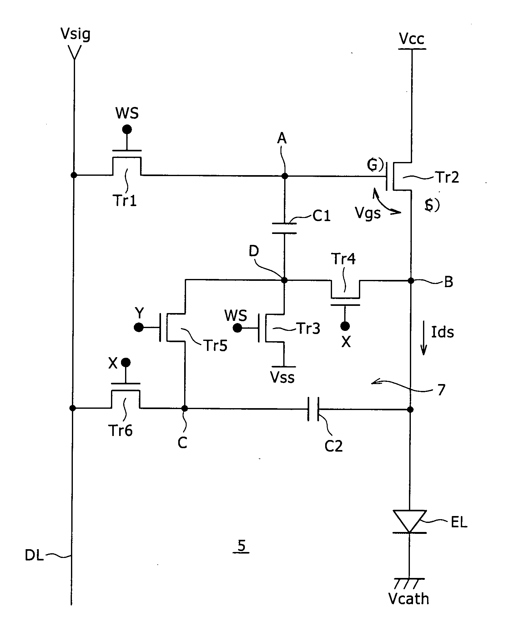
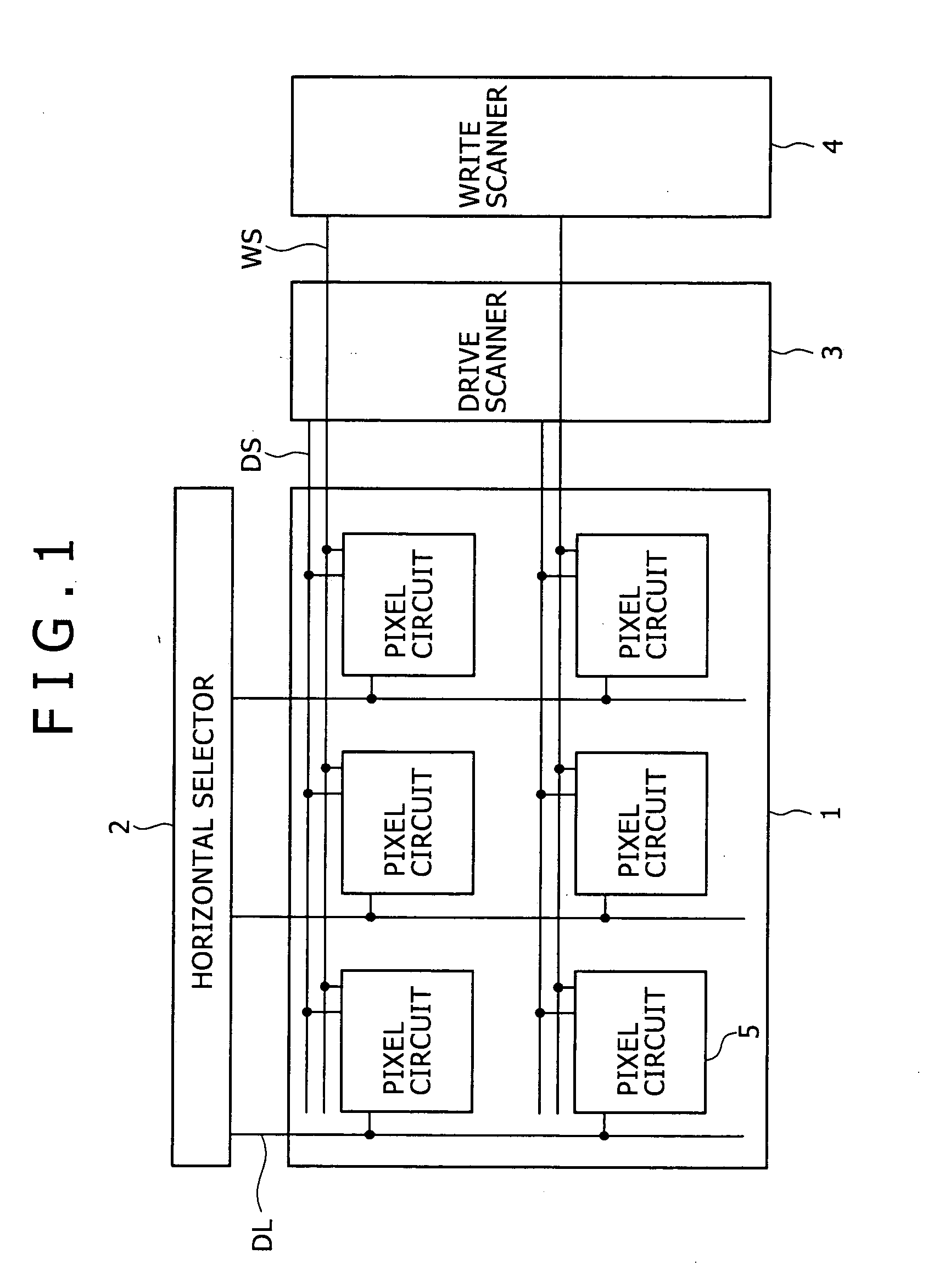
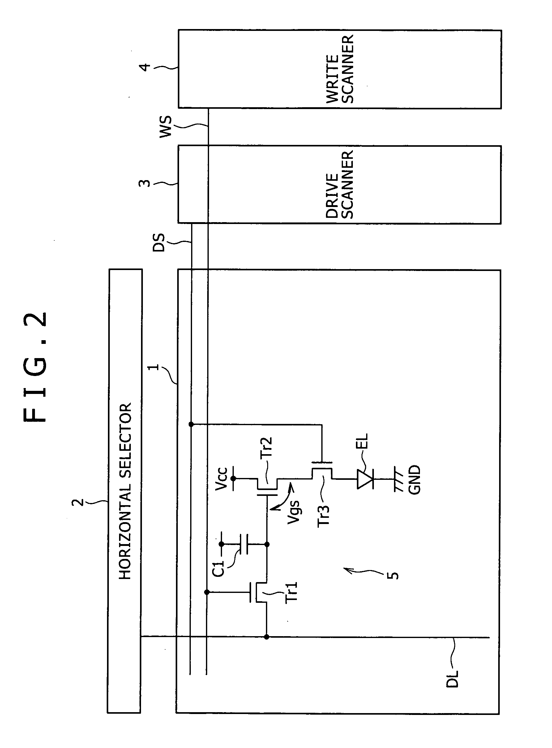
[0052] Preferred embodiments of the present invention will hereinafter be described in detail with reference to the drawings. In order to explain the background of the present invention, a common configuration of an active matrix display device and a pixel circuit included in the active matrix display device will first be described as a reference example with reference to FIG. 1. As shown in the figure, the active matrix display device includes a pixel array 1 as a main part and a peripheral circuit group. The peripheral circuit group includes a horizontal selector 2, a drive scanner 3, a write scanner 4 and the like.

[0053] The pixel array 1 includes scanning lines WS in the form of rows, signal lines DL in the form of columns, and pixel circuits 5 arranged in the form of a matrix at parts where the scanning lines WS intersect the signal lines DL. The signal lines DL are driven by the horizontal selector 2. The scanning lines WS are scanned by the write scanner 4. Incidentally, oth...


PUM


Abstract

A pixel circuit disposed at a part where a scanning line and a signal line intersect each other includes at least an electrooptic element, a drive transistor, a sampling transistor, and a retaining capacitance. The drive transistor has a gate connected to an input node, a source connected to an output node, and a drain connected to a predetermined power supply potential and supplies a driving current to the electrooptic element according to a signal potential retained in the retaining capacitance. The electrooptic element has one terminal connected to the output node and another terminal connected to a predetermined potential. The sampling transistor is connected between the input node and the signal line and operates when selected by the scanning line, samples an input signal from the signal line, and retains the input signal in the retaining capacitance. The retaining capacitance is connected to the input node. The pixel circuit further includes a compensating circuit which detects a decrease in the driving current from a side of the output node, and feeds back a result of detection to a side of the input node, for compensating for a decrease in the driving current which decrease is attendant on a secular change of the drive transistor.

Description

BACKGROUND OF THE INVENTION [0001] The present invention relates to a pixel circuit that performs current driving of a load element disposed in each pixel. The present invention also relates to a display device having such pixel circuits arranged in the form of a matrix, and particularly to a so-called active matrix type display device that controls an amount of current passed through a load element such as an organic EL light emitting element or the like by an insulated gate type electric field effect transistor provided within each pixel circuit. [0002] An image display device, for example a liquid crystal display has a large number of liquid crystal pixels arranged in the form of a matrix, and displays an image by controlling the intensity of transmitted or reflected incident light in each pixel according to image information to be displayed. While this is true for an organic EL display using an organic EL element in a pixel, or the like, the organic EL element is a self light em...

Claims


Application Information

Patent Timeline
Patent Type & Authority Applications(United States)
IPC IPC(8): G09G3/30
CPCG09G3/3233G09G3/3291G09G2300/0417G09G3/3258G09G2300/0852G09G2310/06G09G2320/043G09G2300/0819G09G3/30G09G3/3266G09G2300/0426G09G2310/02G09G2330/028
Inventor UCHINO, KATSUHIDEYAMASHITA, JUNICHI
Owner SONY CORP
Why Eureka
Try Eureka