Liquid crystal display device and method of preventing image sticking thereon

a liquid crystal display device and display device technology, applied in the field of preventing image sticking thereon, can solve the problems of poor view angle characteristic of the twisted nematic liquid crystal display device, and achieve the effect of avoiding image sticking

Active Publication Date: 2006-02-02
AU OPTRONICS CORP
View PDF10 Cites 126 Cited by
  • Summary
  • Abstract
  • Description
  • Claims
  • Application Information

AI Technical Summary

Benefits of technology

[0033] In consideration of the foregoing problem, it is an object of the present invention to provide a liquid crystal display device applying the capacitive coupling HT method for suppressing wash out, which is capable of preventing occurrence of image sticking, and to provide a method of preventing the image sticking.

Problems solved by technology

However, the twisted nematic liquid crystal display device has a disadvantage of a poor view angle characteristic where contrast and color tone vary largely when a screen is viewed from an inclined angle.

Method used


Image

  • Liquid crystal display device and method of preventing image sticking thereon
  • Liquid crystal display device and method of preventing image sticking thereon
  • Liquid crystal display device and method of preventing image sticking thereon

Examples


first embodiment

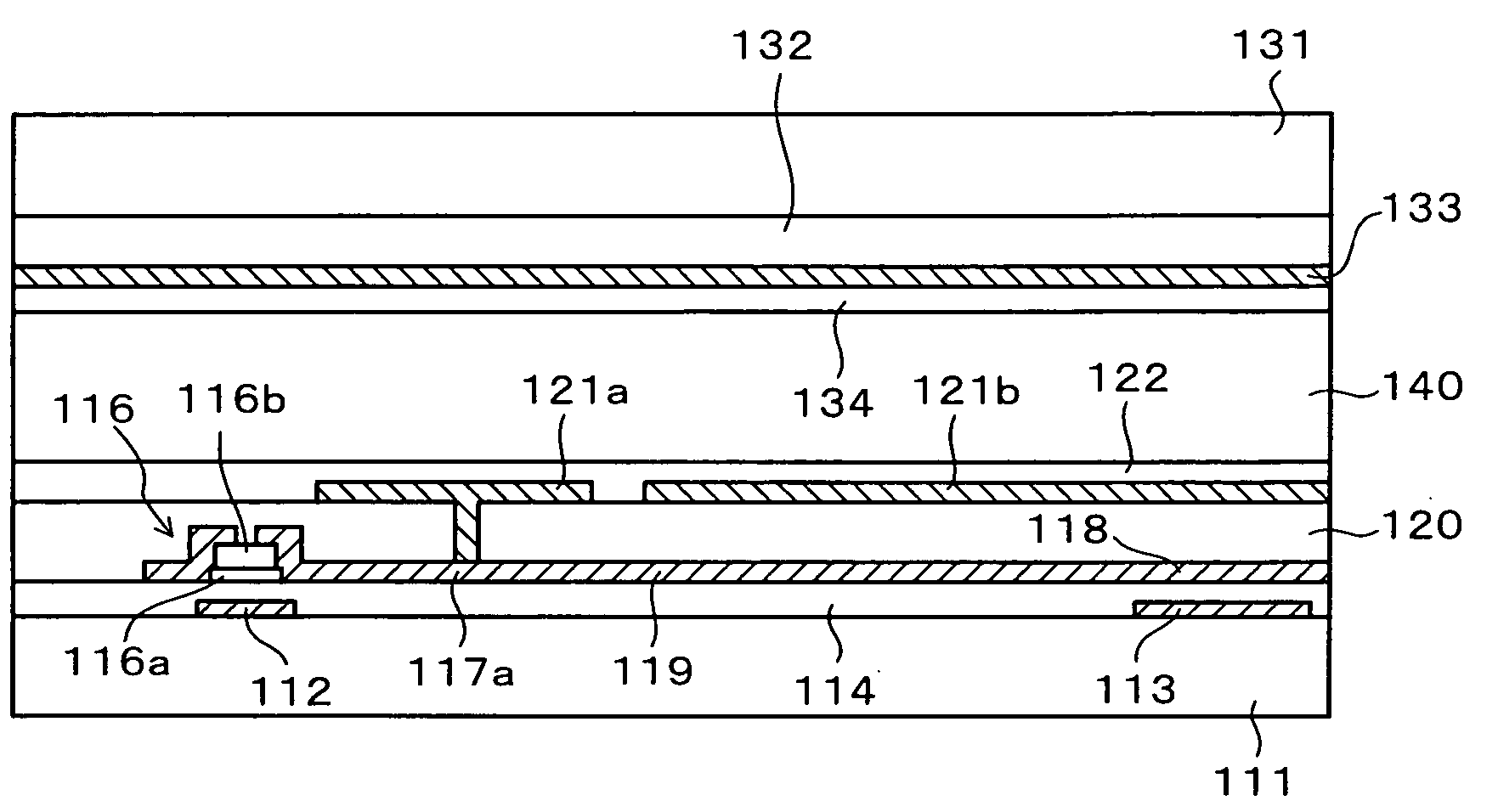
[0118]FIG. 13 is a plan view showing a liquid crystal display device according to a first embodiment of the present invention. Meanwhile, FIG. 14A is a cross-sectional view taken along the VI-VI line in FIG. 13, and FIG. 14B is a cross-sectional view taken along the VII-VII line in FIG. 13.

[0119] On a glass substrate 111 constituting a base of a TFT substrate, there are formed a plurality of gate bus lines 112 extending in a horizontal direction (an X direction) and a plurality of data bus lines 115 extending in a vertical direction (a Y direction). Each rectangular region defined by the gate bus lines 112 and the data bus lines 115 constitutes a picture element region. Meanwhile, on the glass substrate 111, there are formed auxiliary capacitance bus lines 113 disposed parallel to the gate bus lines 112 and intersecting the center of the respective picture element regions.

[0120] A first insulating film 114, which is made of an insulative material such as SiN or SiO2, is formed in ...

second modified example

[0134]FIG. 17 is a plan view showing a liquid crystal display device according to a second modified example of the first embodiment, and FIG. 18 is a cross-sectional view taken along the IX-IX line in FIG. 17. In terms of FIG. 17 and FIG. 18, the same constituents as those illustrated in FIG. 15 and FIG. 16 are designated by the same reference numerals, and detailed description thereof will be omitted.

[0135] In the liquid crystal display device of the second modified example shown in FIG. 17 and FIG. 18, shield patterns 138a and 138b which are formed on the same layer as the sub picture element electrode 136a are disposed between the floating sub picture element electrode 136a and the data bus lines 115. These shield patterns 138a and 138b are electrically connected to the auxiliary capacitance bus line 113 through contact holes 137a and 137b, which are formed on the first and second insulating films 114 and 120, respectively. The auxiliary capacitance bus line 113 is maintained ei...

third modified example

[0137]FIG. 19 is a plan view showing a liquid crystal display device according to a third modified example of the first embodiment, and FIG. 20 is a cross-sectional view taken along the X-X line in FIG. 19. In terms of FIG. 19 and FIG. 20, the same constituents as those illustrated in FIG. 15 and FIG. 16 are designated by the same reference numerals, and detailed description thereof will be omitted.

[0138] In the liquid crystal display device of the third modified example shown in FIG. 19 and FIG. 20, the shield patterns 113a and 113b extending from the auxiliary capacitance bus line 113, and shield patterns 142a and 142b formed on the same layer as the sub picture element electrode 136a are disposed between the floating sub picture element electrode 136a and the data bus lines 115. The shield patterns 142a and 142b are electrically connected to the shield patterns 113a and 113b through contact holes 141a and 141b, which are formed on the first and second insulating films 114 and 12...


PUM

PropertyMeasurementUnit
dielectric constantaaaaaaaaaa
electric potentialaaaaaaaaaa

Abstract

A sub picture element electrode directly connected to a thin film transistor is disposed between a floating sub picture element electrode capacitively coupled to a control electrode and a gate bus line in order to prevent injection of electric charges from the gate bus line to the floating sub picture element electrode. Moreover, a shield pattern electrically connected to an auxiliary capacitance bus line is formed between the floating sub picture element electrode and a data bus line. This shield pattern avoids injection of electric charges from the data bus line to the floating sub picture element electrode.

Description

CROSS-REFERENCE TO RELATED APPLICATIONS [0001] This application is based on and claims priority of Japanese Patent Application No. 2004-220263, filed on Jul. 28, 2004, the entire contents of which are being incorporated herein by reference. BACKGROUND OF THE INVENTION [0002] 1. Field of the Invention [0003] The present invention relates to a liquid crystal display device including a plurality of sub picture element electrodes in one picture element region, and to a method of preventing image sticking thereon. More specifically, the present invention relates to such a liquid crystal display device in which at least one of the sub picture element electrodes is capacitively coupled with a control electrode to which a display voltage is applied, and to a method of preventing image sticking thereon. [0004] 2. Description of the Prior Art [0005] As compared to a cathode ray tube (CRT), liquid crystal display devices have advantages that they are thin, lightweight, as well as have low volt...

Claims


Application Information

Patent Timeline
Patent Type & Authority Applications(United States)
IPC IPC(8): G02F1/136
CPCG02F1/136213G02F2001/136218G02F2001/134354G02F1/134354G02F1/136218B01J47/014C02F1/42C02F1/48C02F1/50C02F1/68C02F5/08
Inventor KAMADA, TSUYOSHISASABAYASHI, TAKASHIUEDA, KAZUYAYOSHIDA, HIDEFUMI
Owner AU OPTRONICS CORP
Why Eureka
Try Eureka