Image sensor package structure and method for fabricating the same

a technology of image sensor and package structure, which is applied in the direction of basic electric elements, electrical equipment, semiconductor devices, etc., can solve the problems of reducing the yield of packaging processes, reducing the utilization of leadless chip carrier packages, and requiring a relative large space, so as to avoid image sensor defects and increase package yield

Inactive Publication Date: 2006-02-02
IND TECH RES INST
View PDF5 Cites 15 Cited by
  • Summary
  • Abstract
  • Description
  • Claims
  • Application Information

AI Technical Summary

Benefits of technology

[0012] A primary object of the present invention is to provide a method for fabricating an image sensor package to prevent particles from falling onto the surface of the image sensor, avoid defects of the image sensor and increase the package yield.
[0013] Another object of the present invention is to provide an image sensor package structure to reduce the size of the package structure, especially the package thickness, make the package structure easy to modularize and prevent particles from falling onto the surface of the image sensor.

Problems solved by technology

Therefore, when an image sensor is packaged with the leadless chip carrier package 30, a relatively large space is required.
And in most cases, this over-sized image sensor limits the utilization of the leadless chip carrier package 30.
As a result, particles will fall onto the surface of the photosensitive unit during the package processes, causing undesirable defects of the image sensor die that decreases the yield of the packaging processes.

Method used


Image

  • Image sensor package structure and method for fabricating the same
  • Image sensor package structure and method for fabricating the same
  • Image sensor package structure and method for fabricating the same

Examples


embodiment 1

abricating an Image Sensor Package

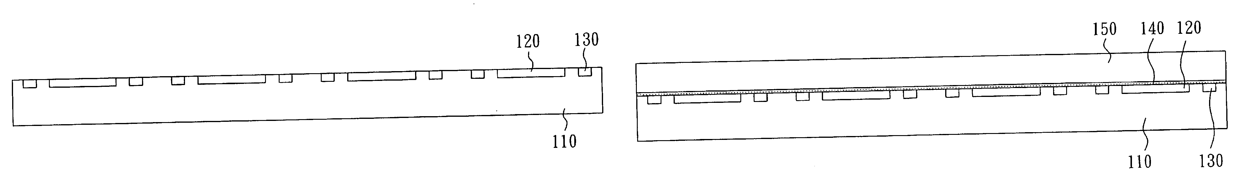
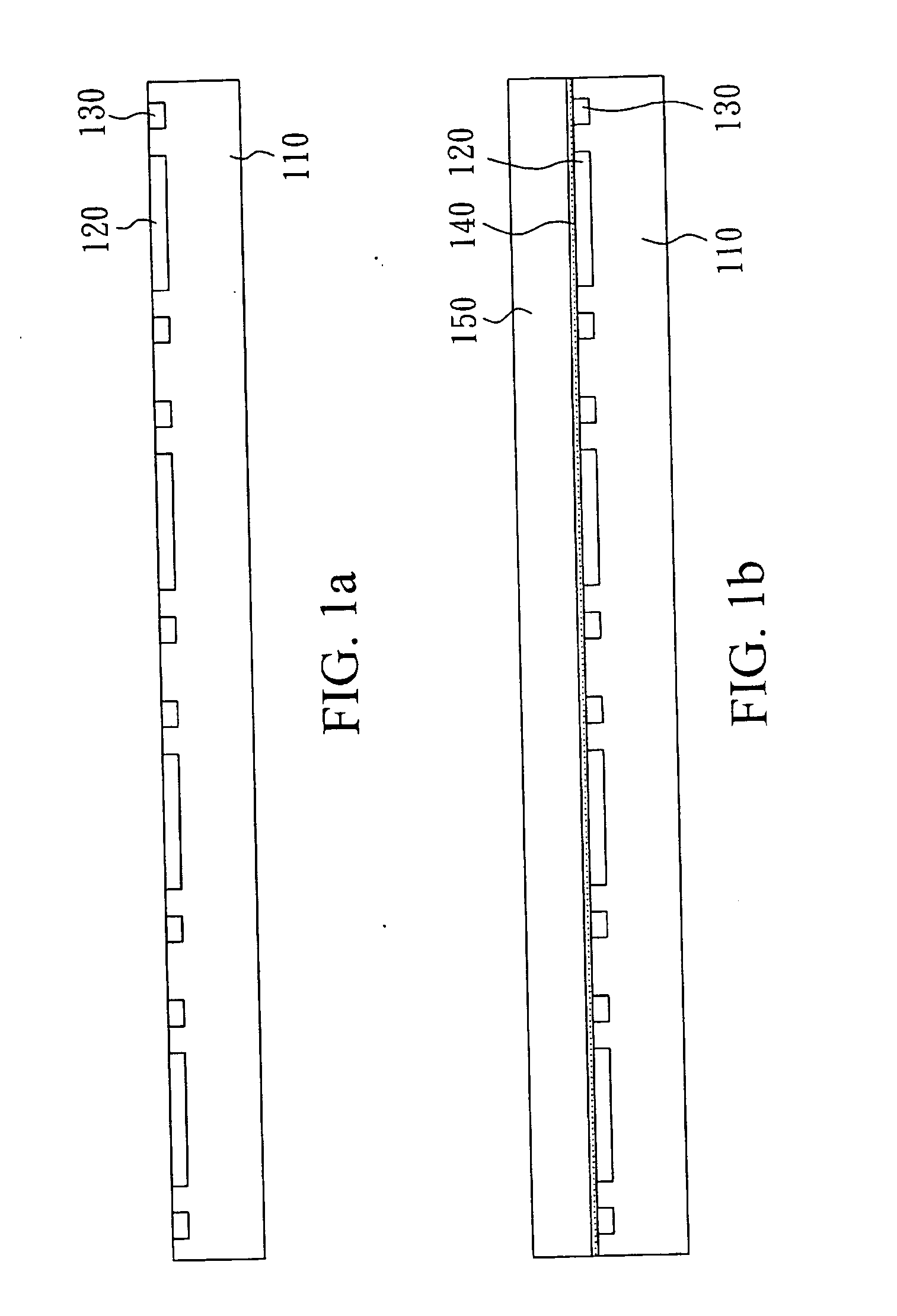
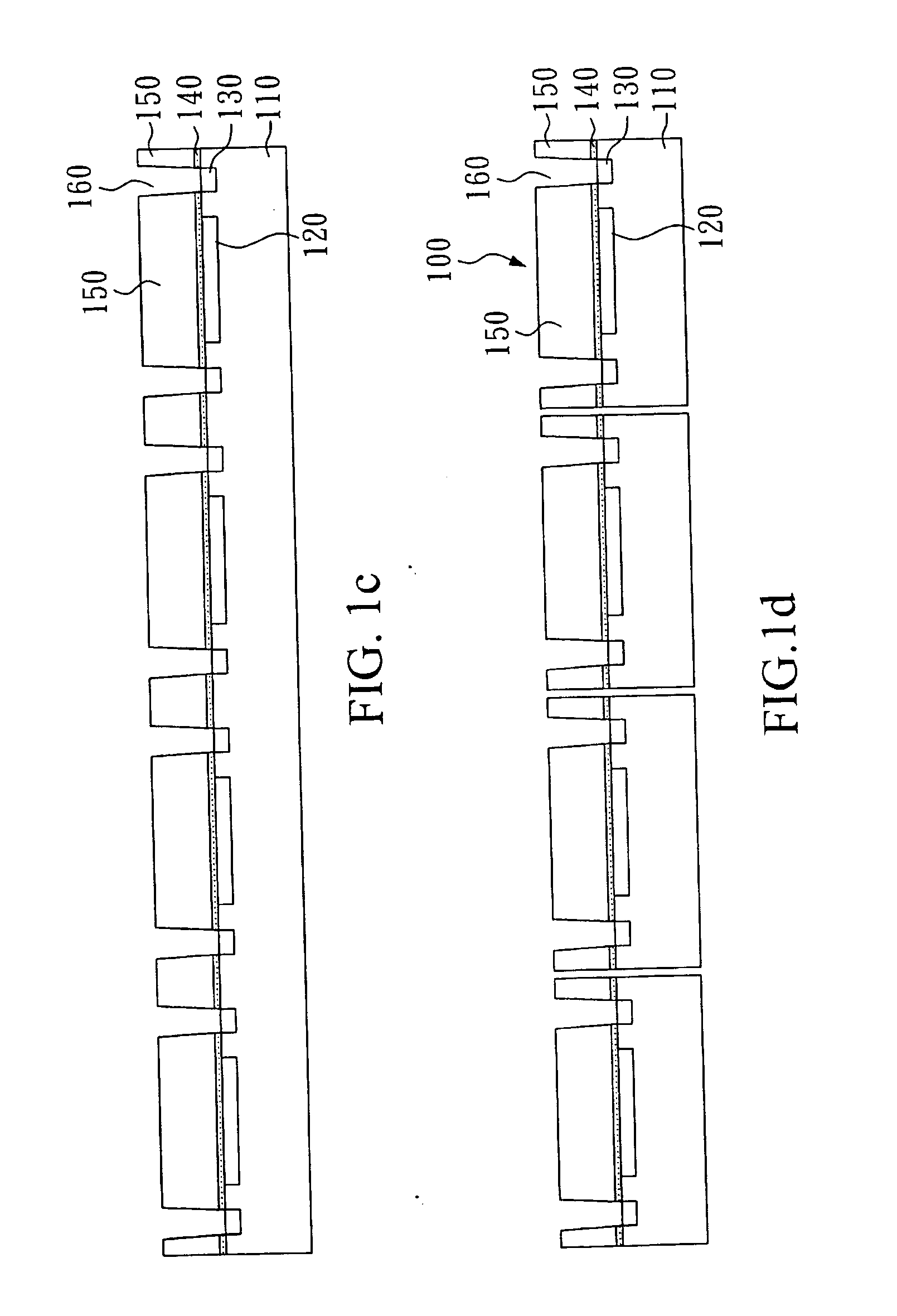
[0029] Referring to FIGS. 1a through 1d, which illustrate a method for fabricating an image sensor package of the present embodiment. As shown in FIG. 1a, a wafer 110 having a plurality of image sensor integrated circuits, each of which has a photosensitive active region 120 and a plurality of first bonding pads 130 is provided. An optical glue 140 is used to have a glass plate 150 adhesively joined to the wafer 110 by partial or whole area so that the photosensitive active region 120 of the image sensor integrated circuit is covered by the glass plate 150, as shown in FIG. 1b. The glass plate 150 can be pre-coated with an anti-reflection layer or any other layer if necessary. As shown in FIG. 1c, a plurality of through holes 160 are formed in the glass plate 150 correspondingly with the first bonding pads 130 of the wafer 110 by laser drilling, so that the first bonding pads 130 can be exposed. Then, the wafer 110 is diced to form a plurality of im...

embodiment 2

abricating an Image Sensor Package

[0031] A method for fabricating an image sensor package is disclosed. First, as shown in FIG. 1a, a wafer 110 having a plurality of image sensor integrated circuits, each of which has a photosensitive active region 120 and a plurality of first bonding pads 130, is provided. As shown in FIG. 1b, an optical glue 140 is used to have a glass plate 150 adhesively joined to the wafer 110 so that the photosensitive active region 120 of the image sensor integrated circuit is covered by the glass plate 150. The glass plate 150 can be pre-coated with an anti-reflection layer or any other layer if necessary. As shown in FIG. 1c, a plurality of through holes 160 are formed in the glass plate 150, correspondingly with the first bonding pads 130 of the wafer 110 by laser drilling, so that the first bonding pads 130 can be exposed. Referring now to FIG. 4a, a conductive material is then filled into the through holes 160 by electroplating. Then, as shown in FIG. 4b...


PUM


Abstract

A method for fabricating an image sensor package is disclosed, comprising: providing a wafer having a plurality of image sensor integrated circuits, each of which has a photosensitive active region and at least one first bonding pad; joining a transparent protecting material to the wafer wherein the photosensitive active region of the image sensor integrated circuit is covered by the transparent protecting material; forming a plurality of through holes in the transparent protecting material, the through holes being correspondingly to the first bonding pad of the wafer to expose the first bonding pad; and dicing the wafer to form a plurality of image sensor integrated circuit components. The method for fabricating an image sensor package of the present invention decreases the defects of the photosensitive active region and reduces the size of the package structure.

Description

BACKGROUND OF THE INVENTION [0001] 1. Field of the Invention [0002] The present invention relates to a semiconductor integrated circuit package structure and method for fabricating the same, and more particularly, to an image sensor package structure and method for fabricating the same. [0003] 2. Description of Related Art [0004]“Multilayered package” is one of the most advanced processes for fabricating semiconductor integrated circuit (IC) products. It can increase the distance between electrodes of an IC die having multilayered package electric circuits, protect the IC die from the internal and external stresses of the package, establish an adequate thermal path for dissipating heat generated by the IC die, and provide an electrical interconnection. The packaging method for the IC dies relates closely to the packaging system used and it dominates the total cost, performance and reliability of the whole package IC die. [0005] Conventional image sensors generally adopt a leadless c...

Claims


Application Information

Patent Timeline
Patent Type & Authority Applications(United States)
IPC IPC(8): H01L21/00
CPCH01L27/14618H01L2224/48091H01L2224/48227H01L2224/48465H01L2924/01078H01L2924/00014H01L2924/00H01L2924/16152
Inventor CHEN, SHOU-LUNGSHEN, LI-CHENG
Owner IND TECH RES INST
Why Eureka
Try Eureka