Methods of forming a capacitors -

a capacitor and capacitor body technology, applied in the field of capacitor formation methods, to achieve the effect of reducing the degree of roundness

a capacitor and capacitor body technology, applied in the field of capacitor formation methods, to achieve the effect of reducing the degree of roundness

US20060024904A1Inactive Publication Date: 2006-02-02MICRON TECH INC

Image

  • Methods of forming a capacitors
 -
  • Methods of forming a capacitors
 -
  • Methods of forming a capacitors
 -

Examples


Embodiment Construction

[0021] This disclosure of the invention is submitted in furtherance of the constitutional purposes of the U.S. Patent Laws ā€œto promote the progress of science and useful artsā€ (Article 1, Section 8).

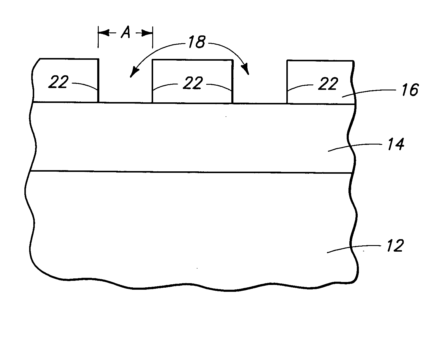
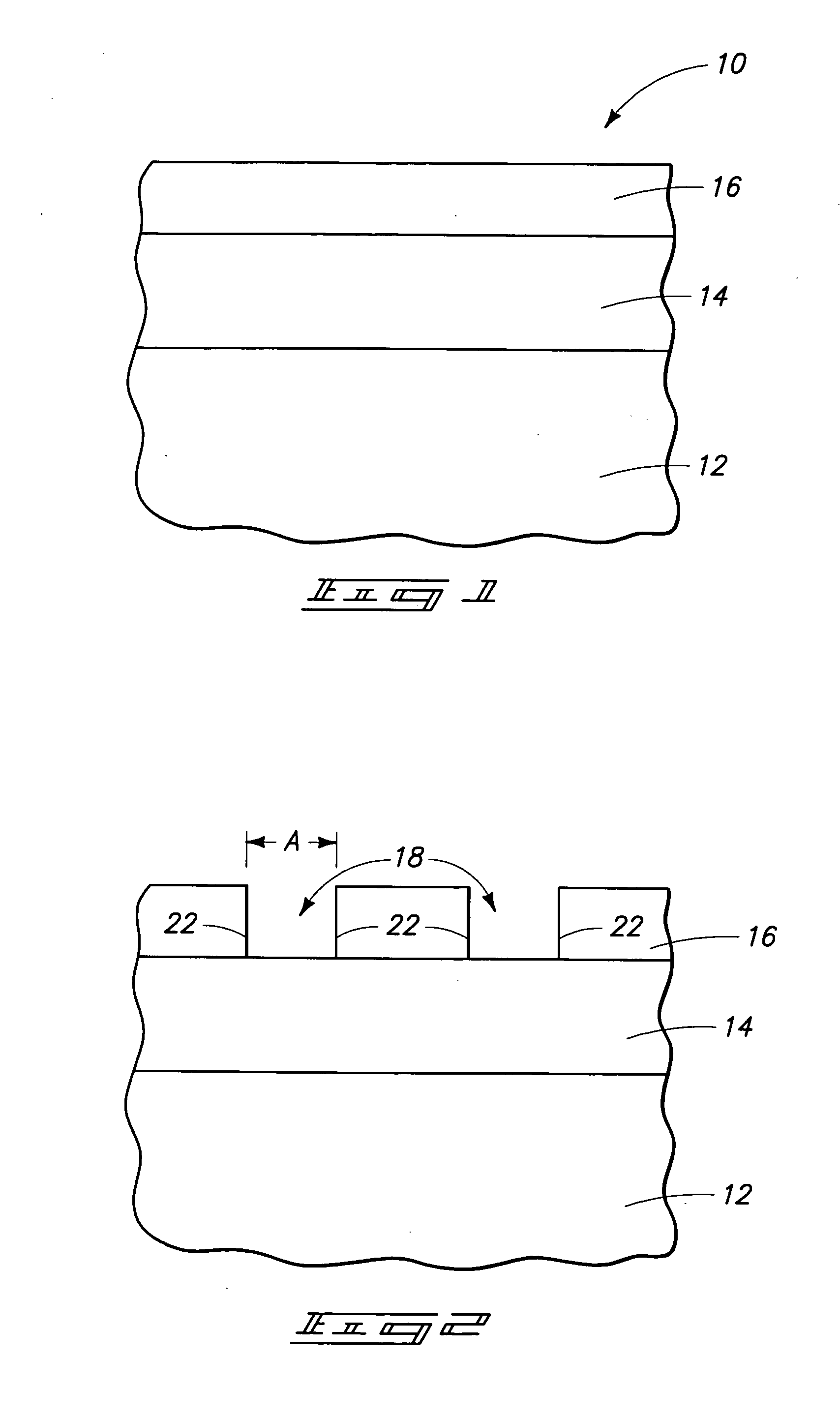
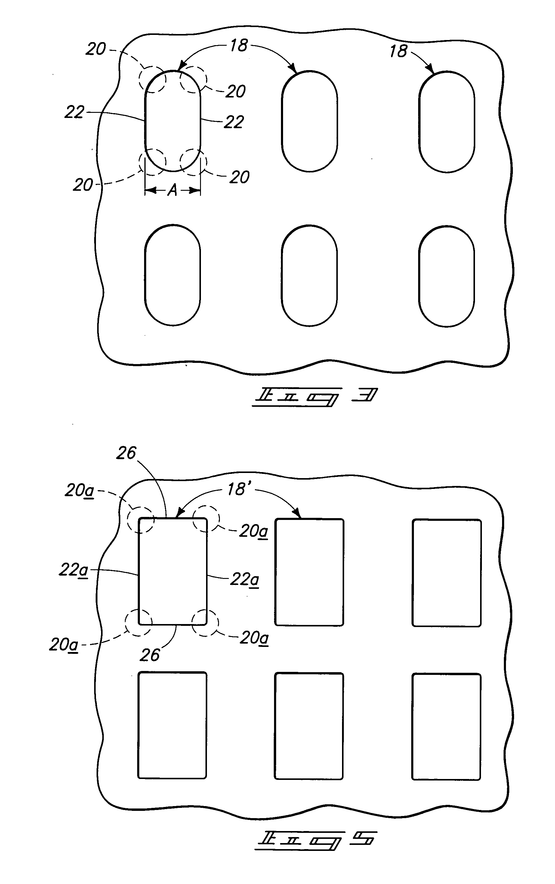
[0022] Preferred embodiment methods of forming capacitors are described with reference to FIGS. 1-18. Referring initially to FIG. 1, a semiconductor substrate is indicated generally with reference numeral 10. In the context of this document, the term ā€œsemiconductor substrateā€ or ā€œsemiconductive substrateā€ is defined to mean any construction comprising semiconductive material, including, but not limited to, bulk semiconductive materials such as a semiconductive wafer (either alone or in assemblies comprising other materials thereon), and semiconductive material layers (either alone or in assemblies comprising other materials). The term ā€œsubstrateā€ refers to any supporting structure, including, but not limited to, the semiconductive substrates described above. Also in the context of this ...


PUM


Abstract

A carbon containing masking layer is patterned to include a plurality of container openings therein having minimum feature dimensions of less than or equal to 0.20 micron. The container openings respectively have at least three peripheral corner areas which are each rounded. The container forming layer is plasma etched through the masking layer openings. In one implementation, such plasma etching uses conditions effective to both a) etch the masking layer to modify shape of the masking layer openings by at least reducing degree of roundness of the at least three corners in the masking layer, and b) form container openings in the container forming layer of the modified shapes. Capacitors comprising container shapes are formed using the container openings in the container forming layer. Other implementations and aspects are disclosed.

Description

RELATED PATENT DATA [0001] This patent resulted from a continuation application of U.S. patent application Ser. No. 10 / 603,242 filed on Jun. 24, 2003, entitled ā€œMethod of Forming a Capacitorā€, naming Aaron R. Wilson as the inventor, and which issued as U.S. Pat. No. 6,933,193 on Aug. 23, 2005, the disclosure of which is incorporated by reference. TECHNICAL FIELD [0002] This invention relates to methods of forming capacitors. BACKGROUND OF THE INVENTION [0003] As DRAMs increase in memory cell density, there is a continuing challenge to maintain sufficiently high storage capacitance despite decreasing cell area. Additionally, there is a continuing goal to further decrease cell area. One principal way of increasing cell capacitance is through cell structure techniques. Such techniques include three-dimensional cell capacitors, such as trenched or stacked capacitors. [0004] One type of capacitor structure forms at least one of the capacitor electrodes into a container-like shape. A suit...

Claims


Application Information

Patent Timeline
02 Feb 2006
Publication
US20060024904A1
IPC
H01L21/20; H01L21/461
CPC
H01L21/31116; H01L21/31144; H01L28/90; H01L27/1085; H01L27/10852; H01L21/76802; H10B12/03; H10B12/033
Inventors
WILSON, AARON R.