Reduction of near field E-M scattering using high impedance coating materials

a coating material and high impedance technology, applied in the direction of transmission, substation equipment, chemistry apparatus and processes, etc., can solve the problems of unfavorable electromagnetic field scattering and more likely to interfere with hearing aid devices, so as to reduce the rf surface wave, and minimize the effect of electromagnetic scattering on the pcb

Inactive Publication Date: 2006-02-09
SONY ERICSSON MOBILE COMM AB
View PDF5 Cites 15 Cited by
  • Summary
  • Abstract
  • Description
  • Claims
  • Application Information

AI Technical Summary

Benefits of technology

[0025] As an example, a thin layer of metal (e.g., aluminum, copper, nickel) is deposited on the surface of a dielectric substrate such as polyethylene, polyimide, or Teflon™. This metallic layer can be on an inner (FIG. 6a), outer (FIG. 6b), or buried (FIG. 6c) within the dielectric substrate. The thin metallic layer allows RF induced currents to spread out over a designated surface area. Similarly, a layer of resistive (electrically lossy) material such as carbon, indium, or ferrites can be applied to a similar dielectric substrate as shown in FIGS. 7a-7c. The resistive material layer provides sufficient attenuation to decrease the RF surface waves and minimize electromagnetic scattering on the PCB. Moreover, since both the metallic and resistive layers can be applied as very thin layers, sufficient transparency can be obtained in desired areas, such as the display area.

Problems solved by technology

When the current reaches an edge of a substrate, undesirable scattering of electromagnetic fields occurs.
The greater the magnitude of scattered fields, the more likely they are to interfere with hearing aid devices.

Method used


Image

  • Reduction of near field E-M scattering using high impedance coating materials
  • Reduction of near field E-M scattering using high impedance coating materials
  • Reduction of near field E-M scattering using high impedance coating materials

Examples


Embodiment Construction

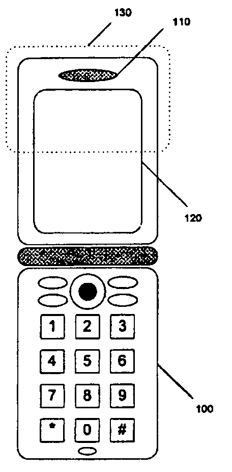
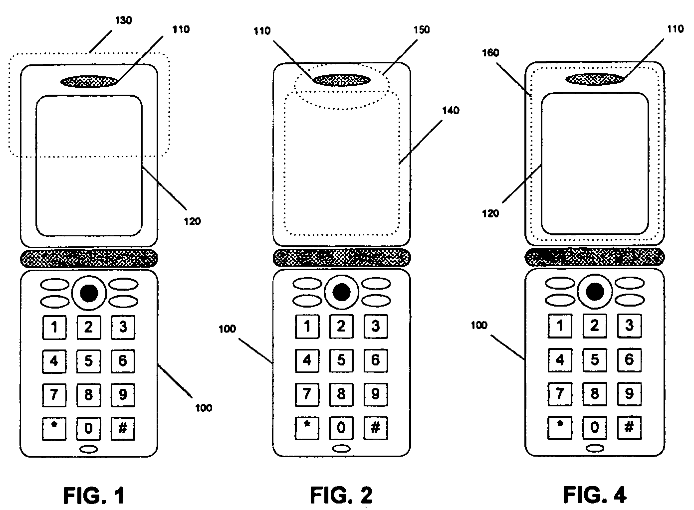
[0004] The present invention employs a high-impedance layer to reduce the effects of E-M scattering at metallic discontinuities. The high-impedance layer can be fabricated using a combination of metallic and resistive materials that are typically used in electro-static discharging (ESD) applications.

[0005] For example, a thin layer of metal (typically aluminum) can be deposited on the surface of a dielectric substrate such as polyethylene. The metallic layer can be applied to the inner surface of the dielectric substrate, the outer surface of the dielectric substrate, or buried within two dielectric substrates. The metallic layer allows RF induced currents to spread out over a designated surface area. Similarly, a layer of resistive material can be applied to the dielectric substrate. The resistive layer provides sufficient attenuation to decrease the RF surface waves and minimize electromagnetic scattering. Furthermore, since these materials can be applied in very thin layers, suf...


PUM

PropertyMeasurementUnit
impedanceaaaaaaaaaa
electro-magneticaaaaaaaaaa
metallicaaaaaaaaaa

Abstract

The present invention selectively uses a high-impedance layer to reduce the effects of E-M scattering at metallic discontinuities. The high-impedance layer can be fabricated using a combination of metallic and resistive materials that are typically used in electro-static discharging (ESD) applications. A thin layer of metal can be deposited on the surface of a dielectric substrate such as polyethylene. This metallic layer can be on an inner, outer, or buried layer of the material. The metallic layer allows the RF induced currents to spread out over a designated surface area. A layer of resistive material can be applied to a similar dielectric layer. The resistive layer provides sufficient attenuation to decrease the RF surface waves and minimize electromagnetic scattering on the printed circuit board (PCB). Furthermore, since the metallic and resistive materials can be applied in very thin layers, sufficient transparency can be preserved in desired areas such as the mobile phone's display region.

Description

BACKGROUND ART [0001] The United States Federal Communications Commission (FCC) is set to enact new regulations in 2005 to improve hearing aid compatibility (HAC) for hearing impaired users of mobile phones. As part of mobile phone HAC assessment, near field components of electromagnetic fields are measured. The components are comprised of electric and magnetic fields. [0002]FIG. 3 illustrates a typical electric field distribution for a flip-type mobile phone having a near field scan area as shown in FIG. 1 and a PCB outline as shown in FIG. 2. The dominant electric fields tend to occur at abrupt discontinuities of metallization such as at the edges of printed circuit boards (PCBs), shield cans, vibrators, and metallization patterns on the assembly. These discontinuities form concentrated electric currents on the metallic substrates that flow toward the edges of a substrate. When the current reaches an edge of a substrate, undesirable scattering of electromagnetic fields occurs. The...

Claims


Application Information

Patent Timeline
Patent Type & Authority Applications(United States)
IPC IPC(8): H04M1/00B32B15/04B32B7/00B32B25/00H01Q1/24H01Q1/52H01Q17/00H04B1/38H04M1/05
CPCH04B1/3838
Inventor HAYES, GERARD JAMES
Owner SONY ERICSSON MOBILE COMM AB
Why Eureka
Try Eureka