High surface quality GaN wafer and method of fabricating same

a technology of gan wafers and wafers, applied in the field of alxgayinzn, can solve the problems of poor device performance, significant thermal stress, internal stress, etc., and achieve the effect of superior surface quality

Inactive Publication Date: 2006-02-09
XU XUEPING +1
View PDF18 Cites 73 Cited by
  • Summary
  • Abstract
  • Description
  • Claims
  • Application Information

AI Technical Summary

Benefits of technology

[0017] The present invention generally relates to AlxGayInzN (wherein 0≦y≦1 and x+y+z=1) having superior surface quality, including in various embodiments, device fabrication surfaces comprising crystallographic plane surfaces and offcuts of such crystallographic plane surfaces, and to methods of fabricating such AlxGayInzN material in wafer form with surfaces suitable for microelectronic and / or optoelectronic device manufacture.

Problems solved by technology

Currently, AlxGayInzN films are grown on non-native substrates such as sapphire or silicon carbide, due to unavailability of high quality AlxGayIn2N substrates.
However, differences in thermal expansion and lattice constants between such foreign substrates and the AlxGayInzN crystals epitaxially grown thereon cause significant thermal stress and internal stress in the grown AlxGayInzN crystals.
Growing on lattice non-matched foreign substrates also causes high density of lattice defects, leading to poor device performance.
However, after mechanical polishing, AlxGayInzN crystals typically have very poor surface quality, with substantial surface and subsurface damage and polishing scratches.
However, such RIE process is unsatisfactory because it is ineffective for removing deeper scratches, and it introduces additional damage by ion bombardment and additional surface irregularities by concomitant contamination, which in turn requires additional cleaning of the GaN wafer in an O2 plasma.

Method used


Image

  • High surface quality GaN wafer and method of fabricating same
  • High surface quality GaN wafer and method of fabricating same
  • High surface quality GaN wafer and method of fabricating same

Examples


example 1

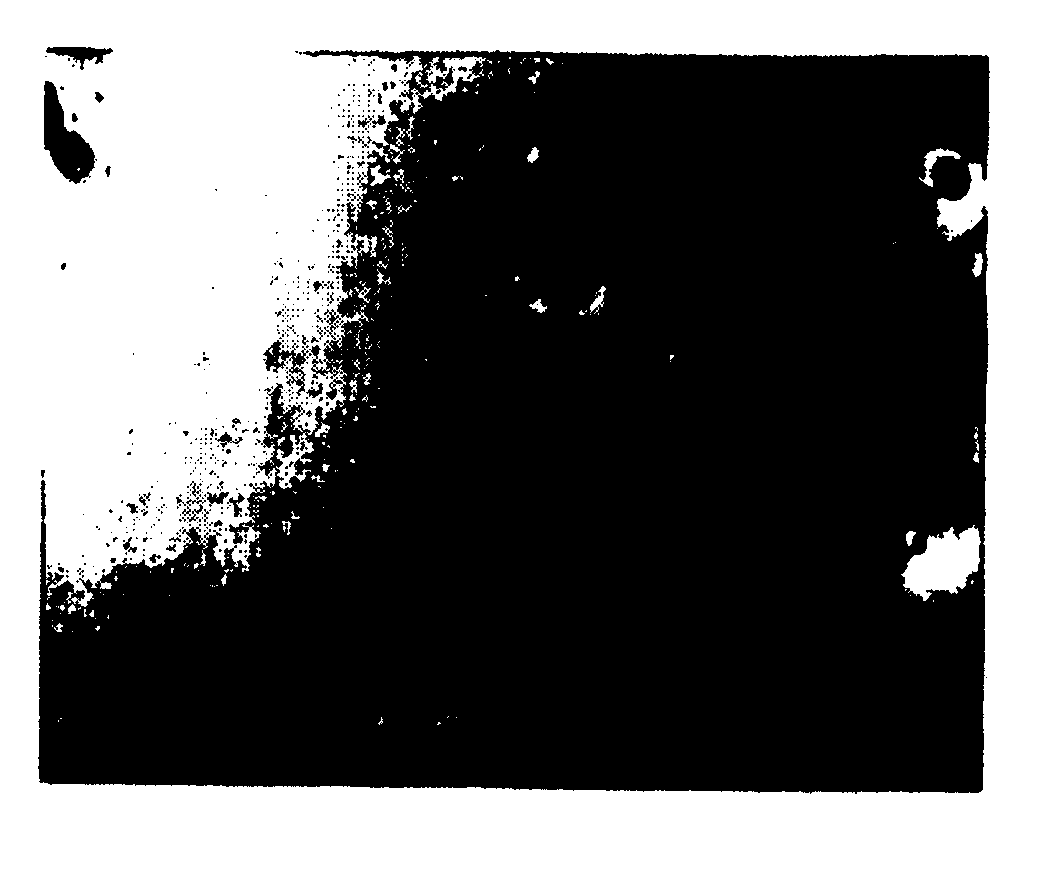
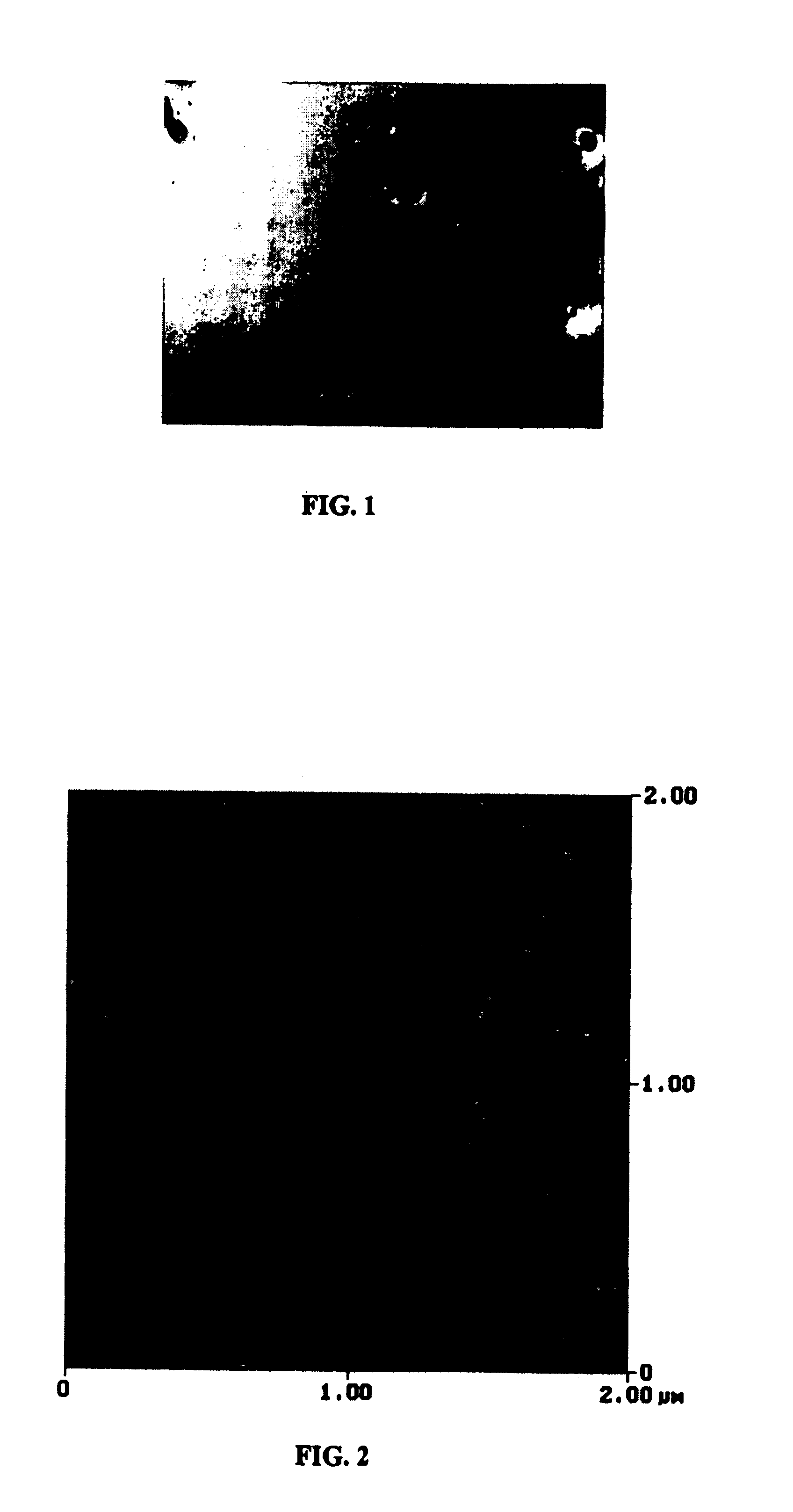
[0136] A GaN film several hundred microns thick was grown on a sapphire substrate by an HVPE process and then separated from the sapphire substrate. The resultantly formed freestanding GaN wafer blank exhibited a textured Ga-surface with a RMS roughness of about 4 nm in a 2×2 μm area.

[0137] The GaN wafer blank was then polished at the Ga-side with an acidic silica slurry without undergoing a lapping process.

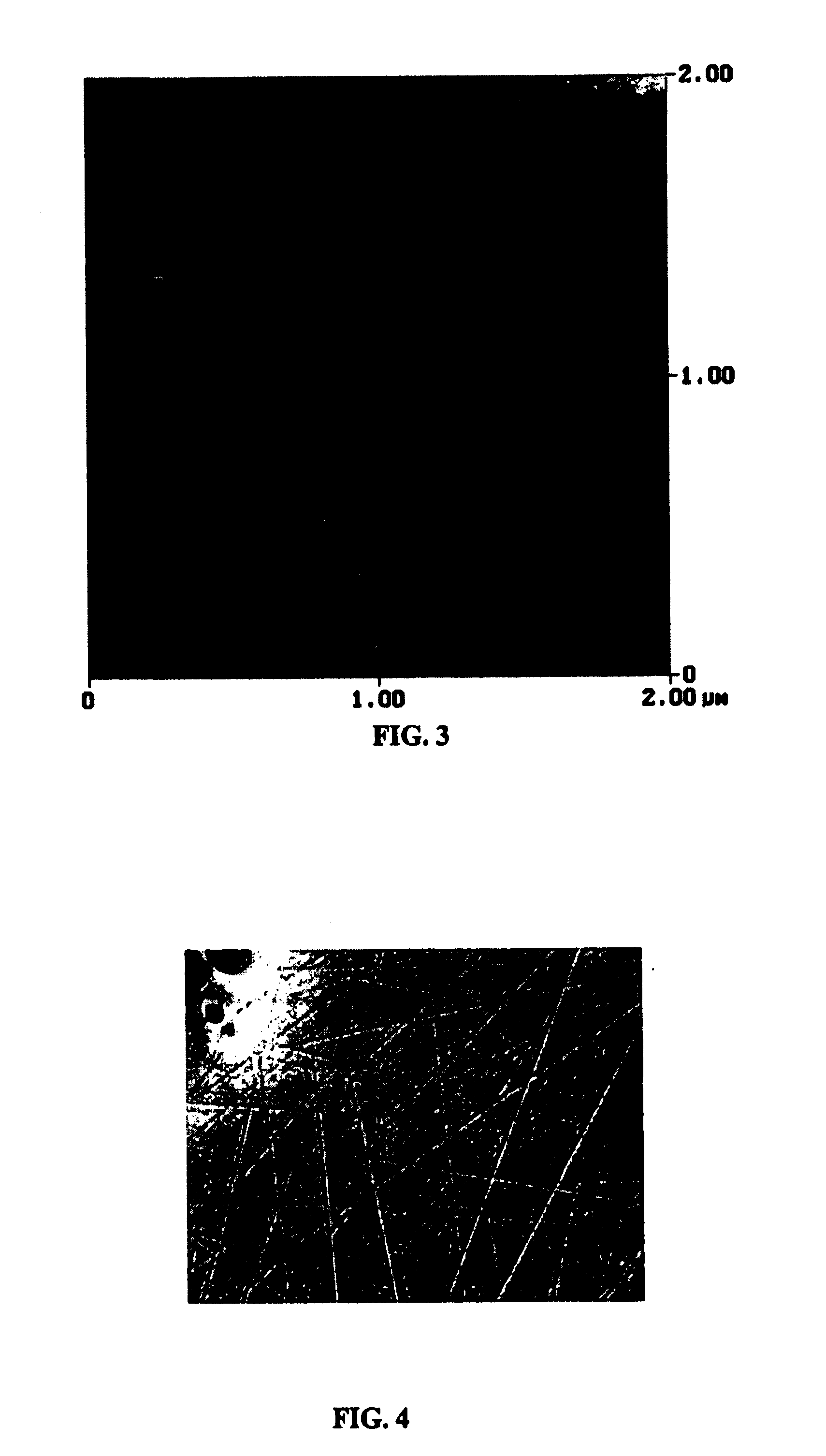
[0138] After polishing, it was observed that the surface morphology of such GaN wafer was greatly improved, with the textured surface being entirely removed. The RMS roughness was reduced to below 0.3 nm in a 2×2 μm2 area.

example 2

[0139] Thick GaN films with thickness in the range from 200-500 microns were grown on 2″ sapphire substrates by an HVPE process. The GaN films then were separated from the sapphire substrate, to yield freestanding GaN wafer blanks.

[0140] Flats for the GaN films were marked as 30° off the sapphire substrate's flat. The GaN wafer blanks then were sized into wafer shapes with diameter of 30, 35, and 40 mm using a particle beam jet. To prevent wafer breakage during wafer sizing, it was preferable to mount the GaN wafer on a glass plate of at least 1 mm thickness, using wax.

[0141] Nine GaN wafers were mounted on a lap fixture with wax with the N-side facing the lap fixture. A steel block was placed on top of each wafer while the wax cooled. The GaN wafers were first lapped on the Ga-side with diamond slurry of 9 μm in diameter on a cast iron lapping plate. Before lapping, a large thickness variation existed between the wafers and within each wafer. After lapping, uniformity of wafer th...

example 3

[0144] Three GaN wafer blanks were mounted on a lap fixture with wax with the Ga-side facing the lap fixture. A steel block was placed on top of each wafer while the wax cooled. The GaN wafers were first lapped on the N-side with diamond slurry of 9 μm in diameter on a Lapmaster 15 lapping machine with cast iron lapping plate until a uniform mat finish was achieved.

[0145] After the N-side was lapped, the GaN wafers were removed from the lap fixture by heating on a hot plate. The wafers were cleaned and mounted on a lap fixture with wax with the N-side facing the lap fixture. A steel block was placed on top of each wafer while the wax cooled. The GaN wafers were lapped on the Ga-side with diamond slurry of 9 μm in diameter on a cast iron lapping plate until a desirable wafer thickness was obtained. Subsequently, the GaN wafers were lapped with diamond slurry of 6 μm in diameter on a copper lapping plate until surface features from the previous lapping step were removed.

[0146] After...


PUM

PropertyMeasurementUnit
surface roughnessaaaaaaaaaa
diameteraaaaaaaaaa
RMS surface roughnessaaaaaaaaaa

Abstract

AlxGayInzN, wherein 0≦x≦1, 0≦y≦1, 0≦z≦1, and x+y+z=1, characterized by a root mean square surface roughness of less than 1 nm in a 10×10 μm2 area. The AlxGayInzN may be in the form of a wafer, which is chemically mechanically polished (CMP) using a CMP slurry comprising abrasive particles, such as silica or alumina, and an acid or a base. High quality AlxGayInzN wafers can be fabricated by steps including lapping, mechanical polishing, and reducing internal stress of said wafer by thermal annealing or chemical etching for further enhancement of its surface quality. CMP processing may be usefully employed to highlight crystal defects of an AlxGayInzN wafer.

Description

CROSS-REFERENCE TO RELATED APPLICATIONS [0001] This is a continuation of U.S. patent application Ser. No. 10 / 272,761 filed Oct. 17, 2002, now allowed, which in turn is a continuation-in-part of U.S. patent application Ser. No. 09 / 877,437 filed Jun. 8, 2001 in the names of Xueping Xu and Robert P. Vaudo, issued Dec. 3, 2002 as U.S. Pat. No. 6,488,767. GOVERNMENT RIGHTS IN INVENTION [0002] The invention disclosed herein includes aspects that were involved in the performance of United States Contract No. DASG60-00-C-0036 issued by the U.S. Army Space and Missile Defense Command and United States Contract No. N00014-00-3-0013 issued by The Office of Naval Research. The government has certain rights in the invention.BACKGROUND OF THE INVENTION [0003] 1. Field of the Invention [0004] This invention relates to AlxGayInzN (wherein 0≦x≦1, 0≦y≦1, 0≦z≦1, and x+y+z=1) having superior surface quality, including in various embodiments, articles formed of such AlxGayInzN material, e.g., in wafer f...

Claims


Application Information

Patent Timeline
Patent Type & Authority Applications(United States)
IPC IPC(8): B32B3/02B32B9/00B32B19/00C30B25/18C09G1/02C30B29/38C30B29/40C30B33/00G01Q30/12G01Q60/00H01L21/304H01L21/306H01L33/00
CPCC09G1/02C09K3/1409C09K3/1463C30B25/02C30B29/403Y10T428/21H01L21/02005H01L21/02019H01L21/02024H01L21/30617H01L33/0075C30B33/00H01L21/20
Inventor XU, XUEPINGVAUDO, ROBERT P.
Owner XU XUEPING
Why Eureka
Try Eureka