

Substrate processing apparatus and method, and gas nozzle for improving purge efficiency
a technology of substrate and processing apparatus, which is applied in the direction of chemical vapor deposition coating, coating, metallic material coating process, etc., can solve the problems of reaction vessel, difficult to reduce the inner volume of reaction vessel, and difficult to reduce the volume of processing space, so as to achieve efficient switching of processing gas and efficient purging
- Summary
- Abstract
- Description
- Claims
- Application Information
AI Technical Summary
Benefits of technology
Problems solved by technology
Method used
Image

Examples
first embodiment
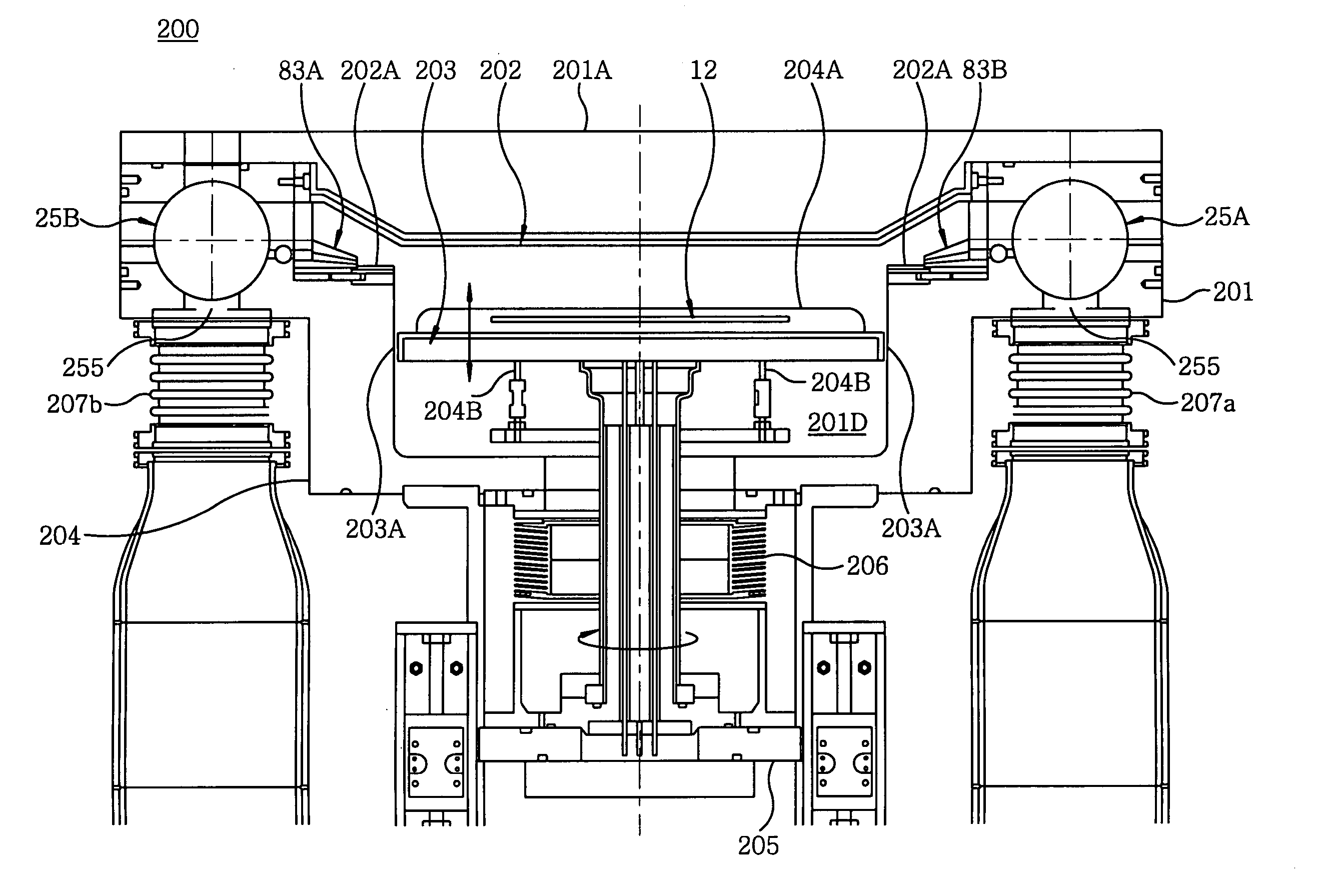
[0054]FIG. 3 shows a configuration of a substrate processing apparatus 200 in accordance with a first embodiment of the present invention; and FIGS. 4A and 4B describe schematic configurations of the substrate processing apparatus 200. Herein, FIG. 4A is a cross sectional view for simplifying FIG. 3; and FIG. 4B is a plane view of FIG. 4A.
[0055] Referring to FIG. 3, the substrate processing apparatus 200 includes an outer vessel 201 made of aluminum alloy, and a cover plate 201A covering the outer vessel 201. In a space formed by the outer vessel 201 and the cover plate 201A, there is installed a reaction vessel 202 forming a processing space.
[0056] Further, a lower part of the processing space is configured as a substrate supporting table 203 for supporting a substrate 12 to be processed, wherein the substrate supporting table 203 is downwardly extended from the outer vessel 201 and installed so as to be able to be vertically moved between an upper and a lower position inside a l...
second embodiment
[0089]FIGS. 10A and 10B describe configurations of the processing gas supply nozzle 83B in accordance with a second embodiment. The same configuration is applied for the processing gas supply nozzle 83A and explanation thereof will be omitted.
[0090] Referring to FIG. 10A, the processing gas supply nozzle 83B in accordance with the second embodiment of the present invention is formed of a hollow housing member 83H whose height gets gradually reduced towards the end portion, wherein the hollow housing member 83H is extended from one end to an opposite end and has a slit shaped injection opening 83b at an end portion thereof.
[0091] As described in FIG. 10B, in the hollow housing member 83H, there is provided a hollow pipe member 83h to be extended continuously from one end of the hollow housing member 83H to the opposite end thereof. In the hollow pipe member 83h, there are formed plural openings 83p along the longitudinal direction thereof. Further, one end of the hollow pipe member...
third embodiment
[0095]FIG. 11 shows a configuration of a substrate processing apparatus 400 using the processing gas supply nozzles 83A and 83B of the prior embodiments, in accordance with a third embodiment of the present invention. In the drawing, parts having substantially the same functions and configurations are designated by the same reference numerals, and their redundant explanations will be omitted unless necessary.
[0096] Referring to FIG. 11, in the present embodiment, an Al2O3 film is formed on the substrate 12 to be processed while the substrate 12 to be processed is not rotated. Therefore, in the substrate processing apparatus 400, the components, such as the rotation unit 205, the magnetic seal working together therewith and the like, can be omitted, so that the configuration thereof can be substantially simplified.
[0097]FIG. 12 describes the formation processing of the Al2O3 film.
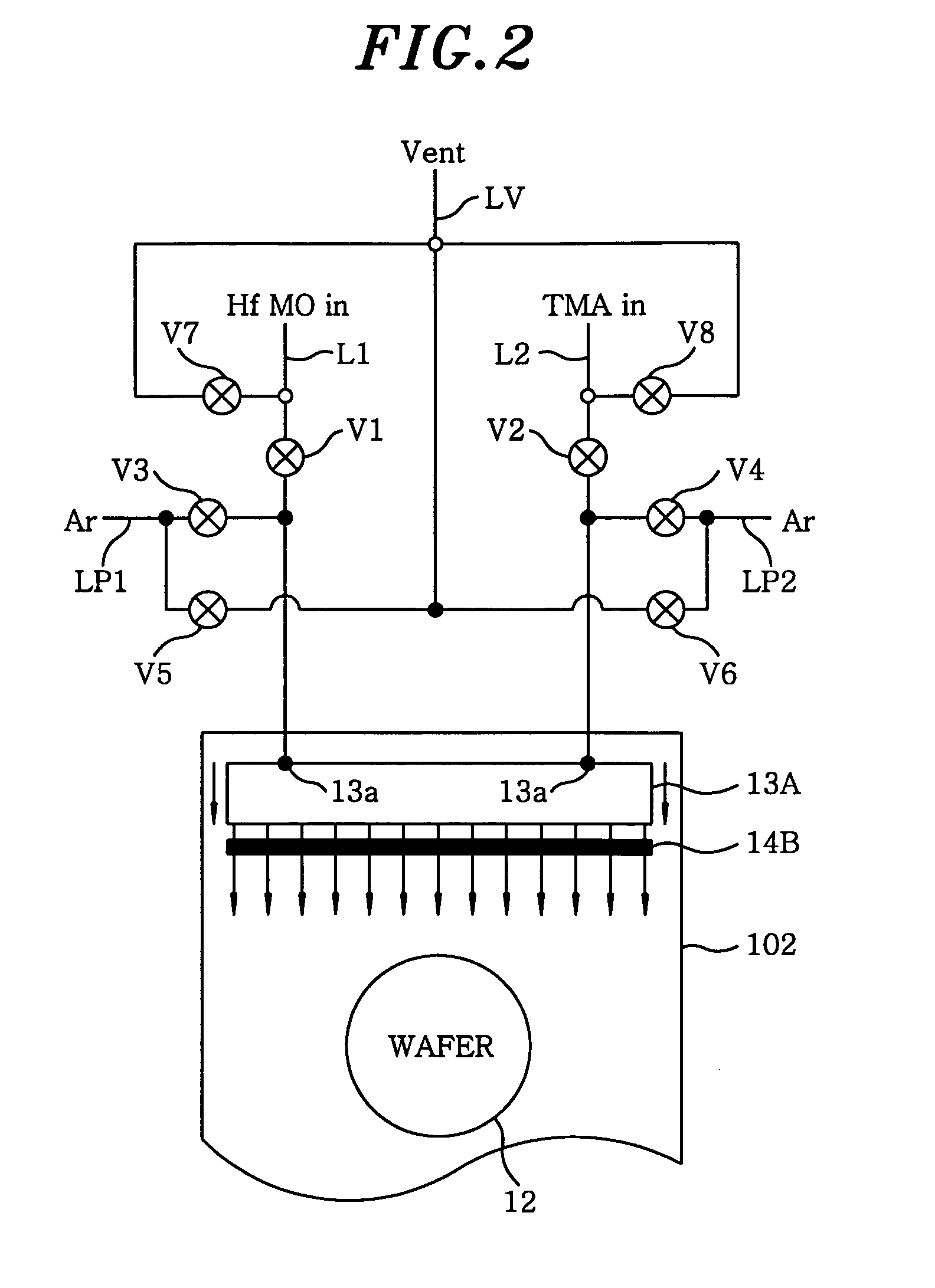
[0098] Referring to FIG. 12, at step 1, the processing gas supply nozzle 83B is closed, and a TMA gas ...
PUM
| Property | Measurement | Unit |
|---|---|---|
| Temperature | aaaaa | aaaaa |
| Time | aaaaa | aaaaa |
| Time | aaaaa | aaaaa |
Abstract
Description
Claims
Application Information