
Pre-emphasis for strobe signals in memory device

a technology of memory device and strobe signal, which is applied in the direction of information storage, static storage, digital storage, etc., can solve the problems of invalid data, inaccurate timing relationship between strobe signal and data signal, and introduction of instability to strobe signal, so as to improve the accuracy of data transfer in memory device.

Active Publication Date: 2006-02-16
MICRON TECH INC
View PDF21 Cites 22 Cited by
  • Summary
  • Abstract
  • Description
  • Claims
  • Application Information

AI Technical Summary

Benefits of technology

[0007] The present invention provides circuits and methods for improving the accuracy of the transfer of data in a memory device.
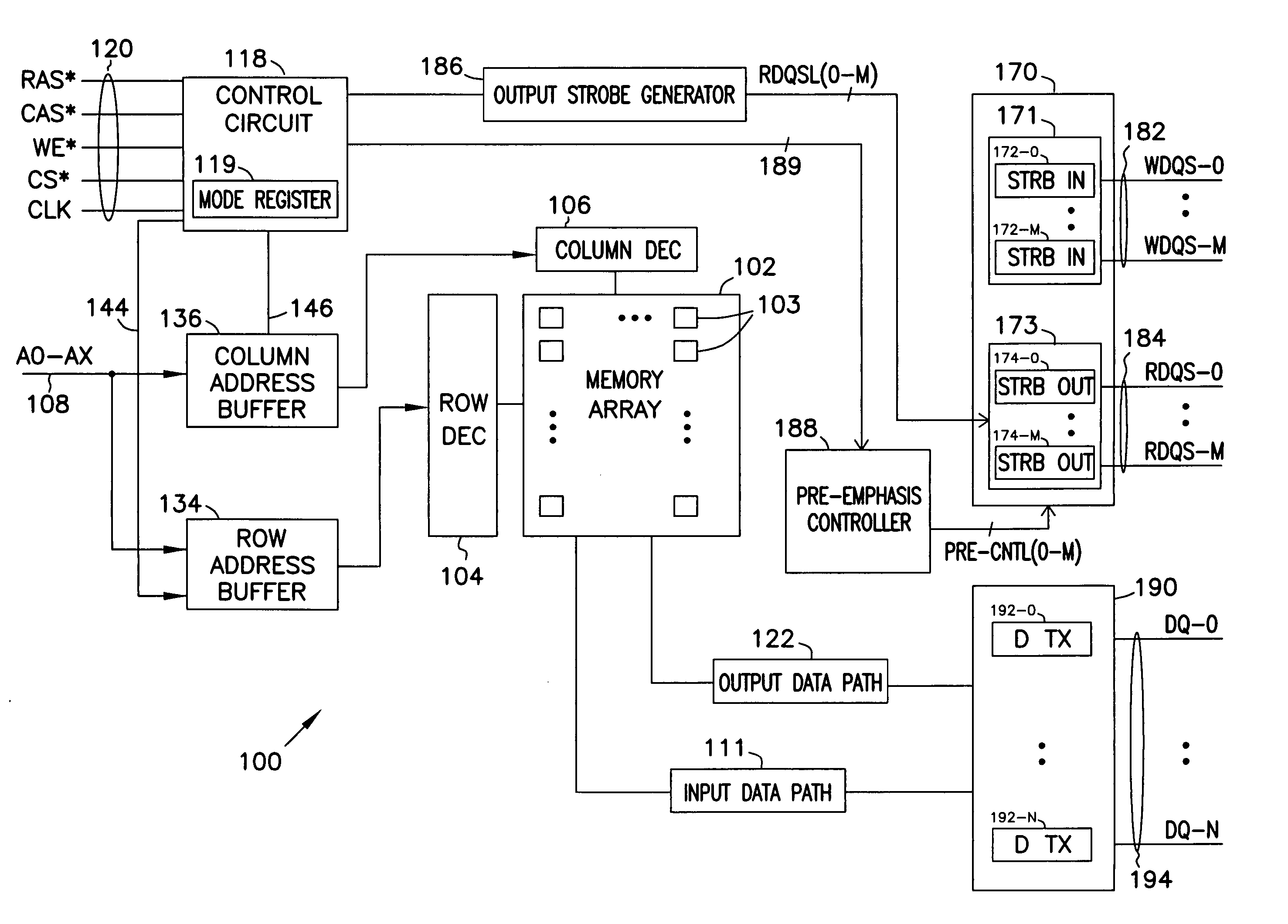
[0008] One aspect includes a memory device having a memory array, a plurality of data terminals, a plurality of strobe terminals, a data transceiver circuit for transferring data signals, and a number of strobe output circuits. Each of the strobe output circuits includes a pair of parallel drivers coupled to a corresponding strobe terminal for outputting a number of strobe signals representing timing information of a number of data signals at the data terminals. The memory device further includes a pre-emphasis controller for influencing signal levels of the strobe signals to reduce any instability at the strobe signals when the strobe signals switch between different signal levels.

Problems solved by technology

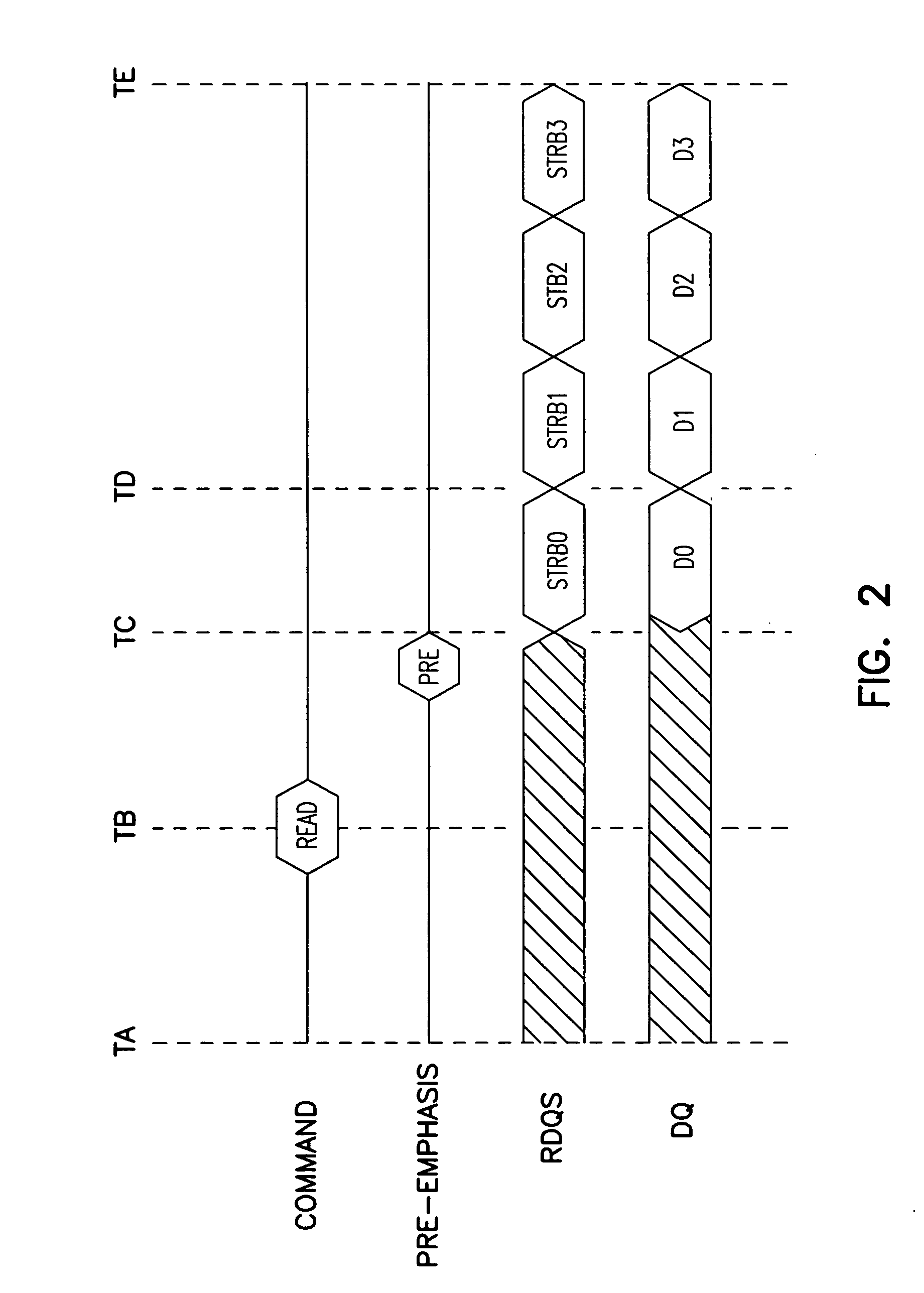
In some cases, switching the strobe signals from one signal level in one mode to another signal level in another mode may introduce instability to the strobe signals at the time of switching.
As a result, the timing relationship between the strobe signals and the data signals may be inaccurate and invalid data may occur.

Method used


Image

  • Pre-emphasis for strobe signals in memory device
  • Pre-emphasis for strobe signals in memory device
  • Pre-emphasis for strobe signals in memory device

Examples


Embodiment Construction

[0023] The following description and the drawings illustrate specific embodiments of the invention sufficiently to enable those skilled in the art to practice the invention. Other embodiments may incorporate structural, logical, electrical, process, and other changes. In the drawings, like numerals describe substantially similar components throughout the several views. Examples merely typify possible variations. Portions and features of some embodiments may be included in or substituted for those of others. The scope of the invention encompasses the claims and all available equivalents.

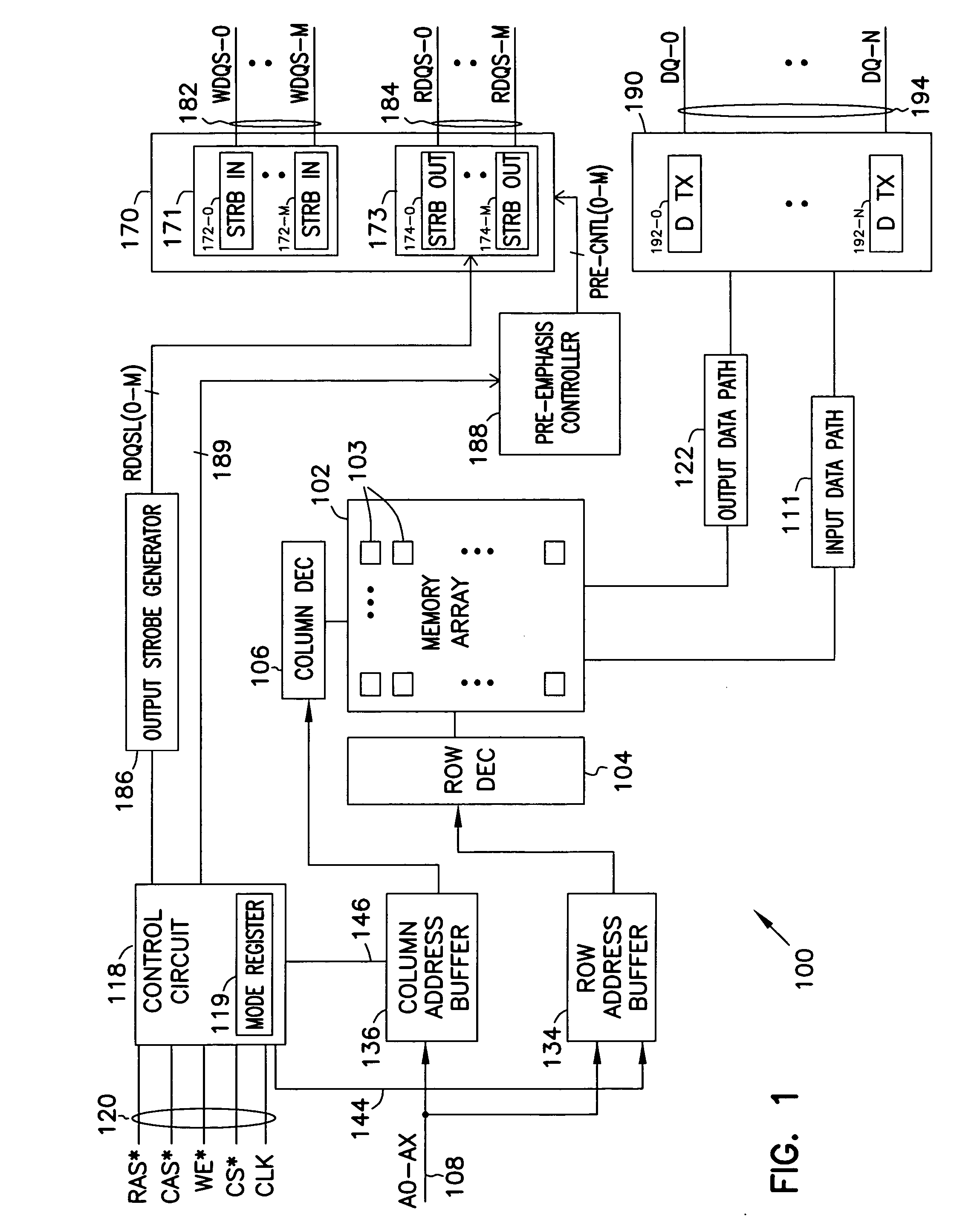
[0024]FIG. 1 shows a memory device according to an embodiment of the invention. Memory device 100 may be a dynamic random access memory (DRAM) device, a static random access memory (SRAM) device, or a flash memory device. Examples of DRAM devices include synchronous DRAM (SDRAM), synchronous graphics random access memory(SGRAM), various generations of double data rate SDRAM (DDR SDRAM), various gener...


PUM


Abstract

A memory device has a number of data terminals for transferring data signals and a number of strobe terminals for transferring strobe signals representing timing information of the data. The strobe terminals have a fixed signal level in an inactive mode of the memory device. The memory further includes a controller for reducing any signal instability of the strobe signals when the memory device switches from the inactive mode to a data transfer mode.

Description

FIELD OF INVENTION [0001] The present invention relates generally to semiconductor devices, more particularly, to transfer of data in memory devices. BACKGROUND [0002] Semiconductors devices such as memory devices reside in many computer and electronic products. Memory devices store data. [0003] Some memory devices have data terminals for transferring data and strobe terminals for transferring strobe signals. The data is transferred based on timing derived from the strobe signals. [0004] The data usually includes many data bits. A strobe signal typically has specified timing reference at which each of the data bits may be accurately transferred. [0005] In some cases, the memory device may be in an inactive mode such that the signal level at the strobe terminals remains at a fixed signal level for a time period. When the memory device switches from the inactive mode to a data transfer mode, the strobe signals at the strobe terminals may switch from the fixed signal level to another s...

Claims


Application Information

Patent Timeline
Patent Type & Authority Applications(United States)
IPC IPC(8): G11C7/00
CPCG11C7/1045G11C7/1066G11C2207/2227G11C7/22G11C7/1093
Inventor CHOI, JOO S.SHARMA, YOGESH
Owner MICRON TECH INC
Learn More