Physical design system and method

a physical design and design technology, applied in the field of integrated circuit and chip design systems, can solve the problems of increasing creativity, effort and expense, and insufficient support of computer-aided design tools for producing manufacturable designs, and achieves the effects of reducing manufacturing cost and risk, reducing layout generation cost and risk, and improving layout data preparation efficiency

Inactive Publication Date: 2006-02-16
GLOBALFOUNDRIES INC
View PDF37 Cites 65 Cited by
  • Summary
  • Abstract
  • Description
  • Claims
  • Application Information

AI Technical Summary

Benefits of technology

[0008] It is yet another purpose of the invention to reduce the cost and risk of layout generation and layout checking;
[0009] It is yet another purpose of the invention to improve the efficiency of layout data preparation;
[0010] It is yet another purpose of the invention to achieve the design goals, matching the final fabricated wafer more exactly to the intended/assumed/modeled design properties and at lower manufacturing cost and risk.
[0011] The present invention relates to a design system for designing c

Problems solved by technology

As semiconductor technology has pushed the limit of physical processes and materials, this assumption is no longer valid.
As a result, increasing creativity, effort and expense has been necessary for design, lithographic patterning and manipulating the design data flow to manufacturin

Method used


Image

  • Physical design system and method
  • Physical design system and method
  • Physical design system and method

Examples


Embodiment Construction

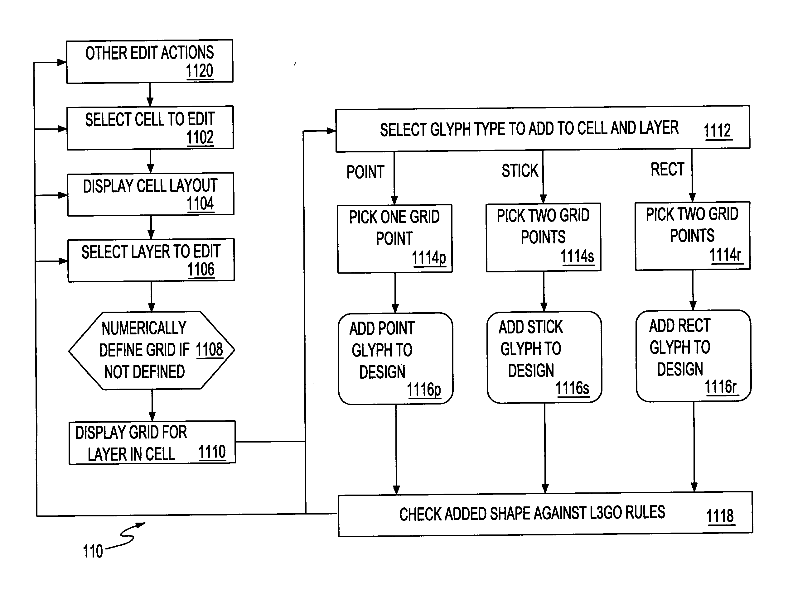
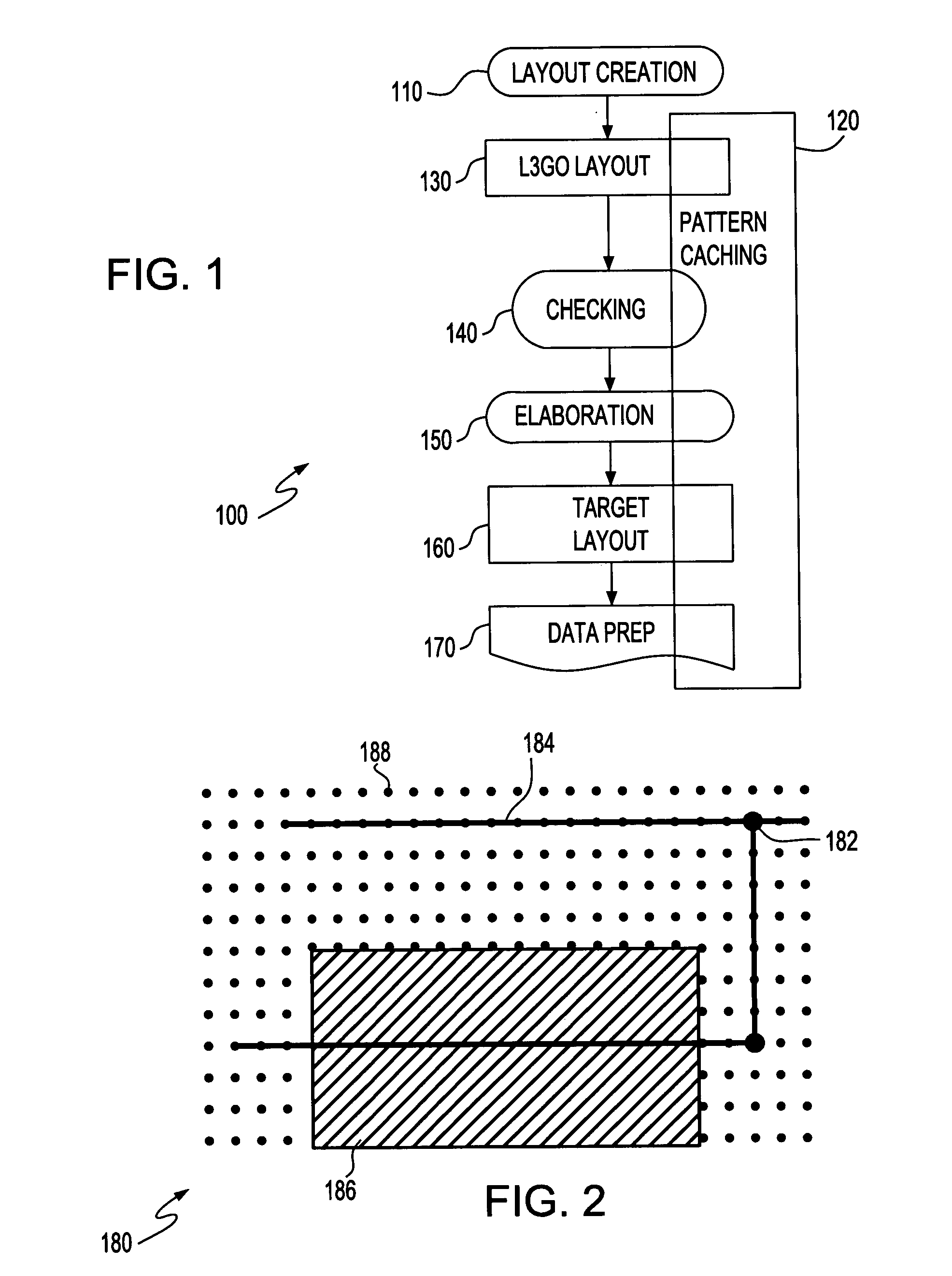
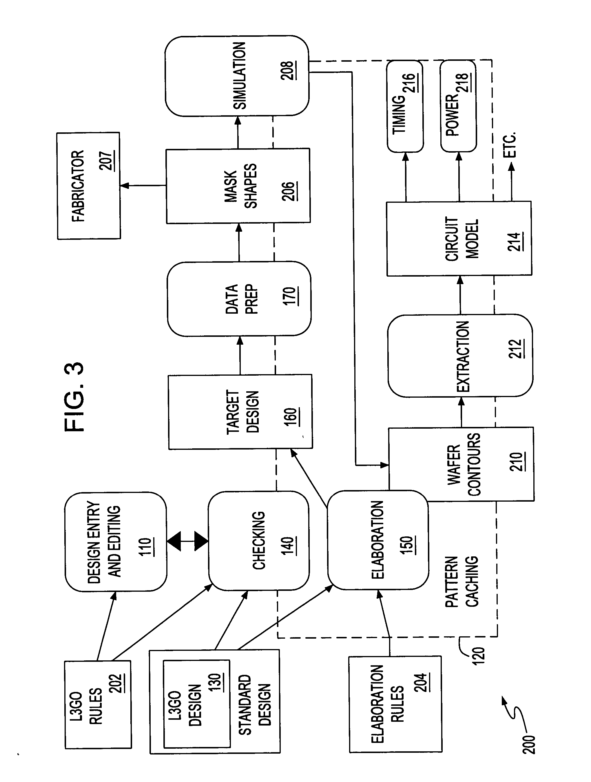
[0021] Turning now to the drawings and, more particularly, FIG. 1 shows a simple example of an integrated circuit (IC) chip, process neutral, physical design flow 100 according to a preferred embodiment of the present invention. A typical state of the art circuit design is provided for physical design 110, primarily in a process neutral grid and glyph representation format. A pattern caching unit 120 monitors and analyzes the process neutral chip physical design flow 100 for optimum handling and workload reduction as the particular grid and glyph representation or layout 130 from physical design 110 traverses the flow. A preferred layout 130 is in a format referred to herein as a layout using gridded glyph geometric objects (L3GO) and referred to a L3GO layout. A L3GO layout 130 is, essentially, an extension to a conventional design. Conventional physical design layouts are organized in cells, layers, transforms and represented solely by polygonal shapes with coordinates in database...


PUM


Abstract

A design system for designing complex integrated circuits (ICs), a method of IC design and program product therefor. A layout unit receives a circuit description representing portions in a grid and glyph format. A checking unit checks grid and glyph portions of the design. An elaboration unit generates a target layout from the checked design. A data prep unit prepares the target layout for mask making. A pattern caching unit selectively replaces portions of the design with previously cached results for improved design efficiency.

Description

BACKGROUND OF THE INVENTION [0001] 1. Field of the Invention [0002] The present invention is related to integrated circuit (IC) and chip design systems and more particularly to computer aided design (CAD) systems for designing ICs and IC chips. [0003] 2. Background Description [0004] Semiconductor technology and chip manufacturing advances have resulted in a steady decrease of chip feature size to increase on-chip circuit switching frequency (circuit performance) and the number of transistors (circuit density). Typical semiconductor integrated circuit (IC) chips are multilayered units with circuit layers stacked such that layer features overlay one another to form individual devices and connect devices together. Individual layers normally are patterned lithographically using well known photolithographic techniques as applied to semiconductor manufacturing. Normally, a chip designer creates an electrical or logic representation of a new chip that is converted to a chip / circuit layout...

Claims


Application Information

Patent Timeline
IPC IPC(8): G06F17/50
CPCG06F17/5072G06F17/5081G06F17/5009G06F30/392G06F30/398G06F30/20
Inventor COHN, JOHN M.CULP, JAMES A.FINKLER, ULRICH A.HENG, FOOK-LUENLAVIN, MARK A.LEE, JIN FUWLIEBMANN, LARS W.NORTHROP, GREGORY A.SEONG, NAKGEUONSINGH, RAMA N.STOK, LEONWOLTGENS, PIETER J.
Owner GLOBALFOUNDRIES INC
Why Eureka
Try Eureka