Gallium-nitride based light emitting diode structure with enhanced light illuminance

a technology of light emitting diodes and gallium nitride, which is applied in the direction of basic electric elements, electrical apparatus, semiconductor devices, etc., can solve the problems of limited and the effectiveness of its application is not very satisfactory, so as to achieve the effect of significantly increasing the light illuminance and light transmittance efficiency of multi-quantum-well light emitting diodes

Inactive Publication Date: 2006-02-23
FORMOSA EPITAXY INCORPORATION +1
View PDF1 Cites 236 Cited by
  • Summary
  • Abstract
  • Description
  • Claims
  • Application Information

AI Technical Summary

Benefits of technology

[0012] The special design multi-quantum-well light emitting diode according to the present invention is characterized in that it does not make use of Ni/Au as the material for its top layer as in the prior art, but instead it utilizes ITO as the material for its top transparent contact layer. Therefore, according to the experiment data as shown in FIG. 2, the light transmittance of the transparent con

Problems solved by technology

However, its light illuminance and light transmittance efficiency are restricted by the property of its top transparent contact layer, and its light transmittance at present can only reach 62% at most in the visible light spectrum.
Therefore, the effectiveness of its application

Method used


Image

  • Gallium-nitride based light emitting diode structure with enhanced light illuminance
  • Gallium-nitride based light emitting diode structure with enhanced light illuminance
  • Gallium-nitride based light emitting diode structure with enhanced light illuminance

Examples


embodiment 1

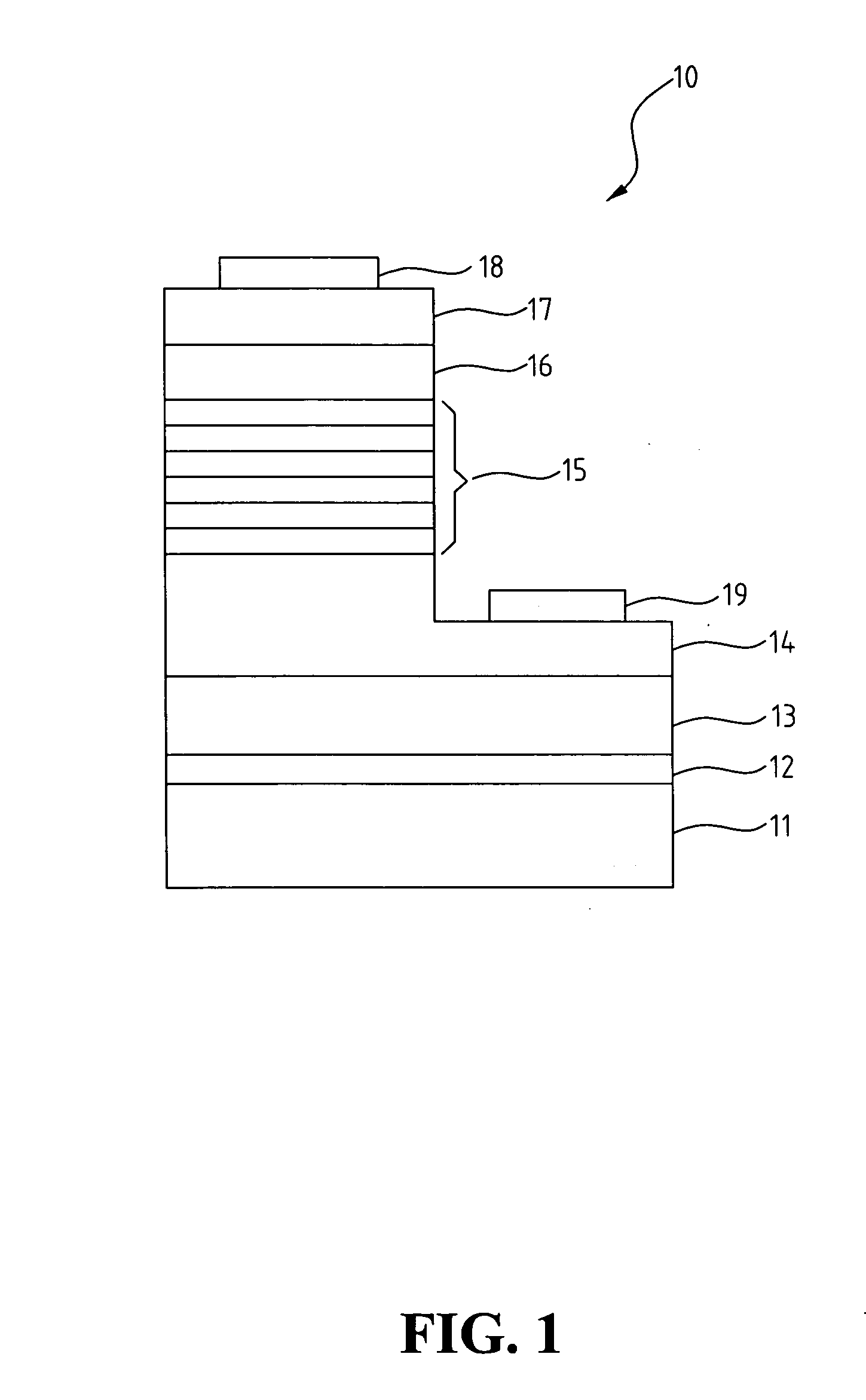
[0021]FIG. 3 shows a gallium-nitride based light emitting diode structure 30 with enhanced light illuminance according to the first embodiment of the present invention, comprising: substrate 31, buffer layer 32, n-type gallium nitride (GaN) layer 33, active light-emitting-layer 34, p-type cladding layer 35, p-type contact layer 36, barrier buffer layer 37, transparent contact layer 38, and n-type electrode layer 39.

[0022] The bottom layer of the structure is substrate 31, and it is made of Sapphire. And next ,the buffer layer 32 is formed on substrate 31, and it is made of aluminum-gallium-indium-nitride (Al1-x-yGaxInyN) wherein 0≦x≦1, 0≦y≦1 and x+y≦1. The n-type gallium-nitride (GaN) layer 33 is formed on buffer layer 32. The active light-emitting-layer 34 is formed on n-type gallium-nitride (GaN) layer 33, and it is made of indium-gallium-nitride (InGaN). And next, the p-type cladding layer 35 is formed on active light-emitting-layer 34, and it is made of Mg-doped aluminum-indium...

embodiment 2

[0024]FIG. 4 shows a gallium-nitride based light emitting diode structure 40 with enhanced light illuminance according to a second embodiment of the present invention, comprising: substrate 41, buffer layer 42, n-type gallium-nitride (GaN) layer 43, active light-emitting-layer 44, p-type cladding layer 45, p-type contact layer 46, short-period super-lattice barrier buffer layer 47, transparent contact layer 48, and n-type electrode layer 49.

[0025] The bottom layer of the structure is substrate 41, and it is made of Sapphire. And next, the buffer layer 42 is formed on substrate 41, and it is made of aluminum-gallium-indium-nitride (Al1-x-yGaxInyN), wherein 0≦x≦1, 0≦y≦1 and x+y≦1. Then, the n-type gallium-nitride (GaN) layer 43 is formed on buffer layer 42. And then, the active light-emitting-layer 44 is formed on n-type gallium nitride (GaN) layer 43, and it is made of indium-gallium nitride (InGaN). And next the p-type cladding layer 45 is formed on active light-emitting-layer 44, ...

embodiment 3

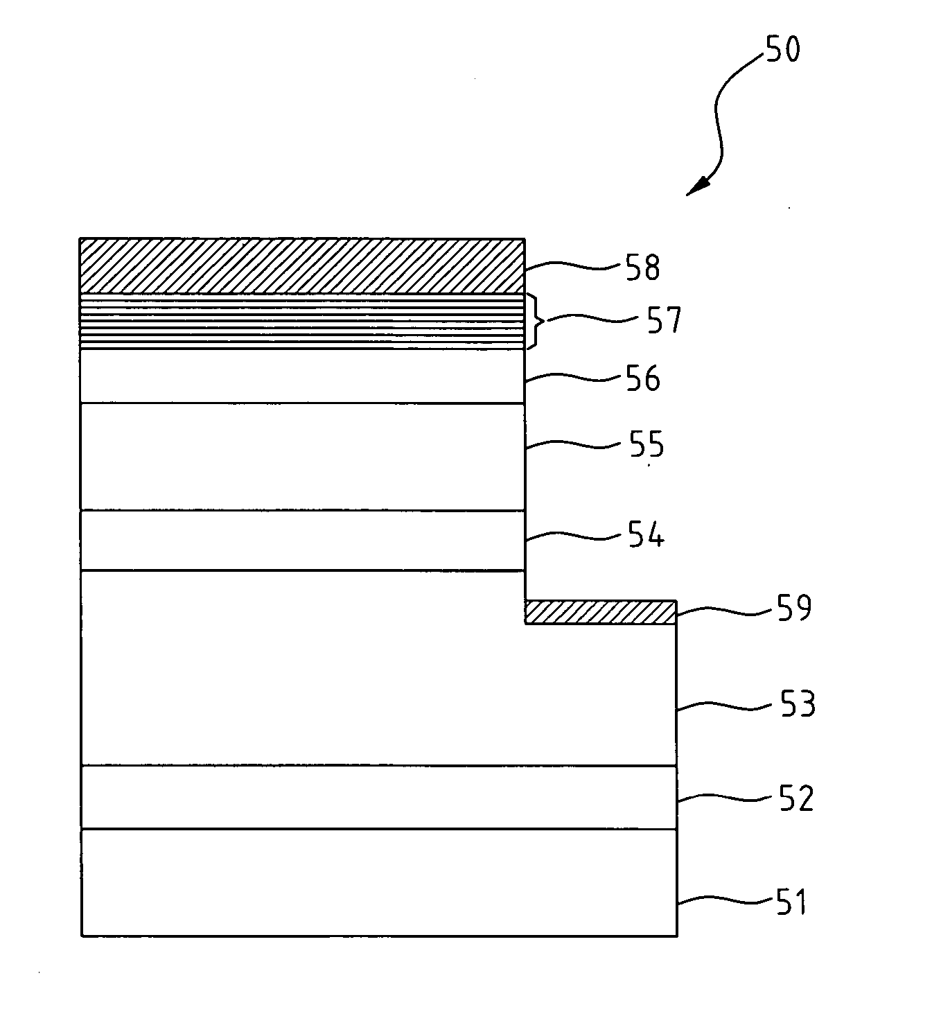
[0027]FIG. 5 shows a gallium-nitride based light emitting diode structure 50 with enhanced light illuminance according to a third embodiment of the present invention, comprising: substrate 51, buffer layer 52, n-type gallium nitride (GaN) layer 53, active light-emitting-layer 54, p-type cladding layer 55, p-type contact layer 56, short-period super-lattice barrier buffer layer 57, transparent contact layer 58, and n-type electrode layer 59.

[0028] The bottom layer of the structure is substrate 51, and it is made of Sapphire. And next, the buffer layer 52 is formed on substrate 51, and it is made of aluminum-gallium-indium-nitride (Al1-x-yGaxInyN), wherein 0≦x≦1, 0≦y≦1 and x+y≦1. Then, the n-type gallium nitride (GaN) layer 53 is formed on buffer layer 52. And then, the active light-emitting-layer 54 is formed on n-type gallium nitride (GaN) layer 53, and it is made of indium-gallium nitride (InGaN). And next, the p-type cladding layer 55 is formed on active light-emitting-layer 54, ...


PUM


Abstract

Disclosed is a multi-quantum-well light emitting diode, which makes enormous adjustments and improvements over the conventional light emitting diode, and further utilizes a transparent contact layer of better transmittance efficiency, so as to significantly raise the illuminance of this light emitting diode and its light emission efficiency. The multi-quantum-well light emitting diode has a structure including: substrate, buffer layer, n-type gallium-nitride layer, active light-emitting-layer, p-type cladding layer, p-type contact layer, barrier buffer layer, transparent contact layer, and the n-type electrode layer.

Description

BACKGROUND OF THE INVENTION [0001] 1. Field of the Invention [0002] The present invention relates to the gallium-nitride (GaN) based light-emitting-diode (LED) structure, and in particular to the gallium-nitride (GaN) based light emitting diode which achieves the increased light transmittance and enhanced light illuminance by means of its top transmittance contact layer using ITO (indium-tin-oxide) as its material. [0003] 2. The Prior Arts [0004] It is known, the indium-gallium-nitride (InGaN) / gallium-nitride (GaN) multi-quantum well (MQW) LED is usually used in the prior art as the light emitting device. It has been widely utilized in the various functions and applications of static display, such as, in the clocks / watches, display screens, and advertisement panels, etc for displaying digits and / or images. However, its light illuminance and light transmittance efficiency are restricted by the property of its top transparent contact layer, and its light transmittance at present can o...

Claims


Application Information

Patent Timeline
IPC IPC(8): H01L33/00H01L29/18H01L33/04H01L33/14H01L33/32H01L33/42
CPCH01L33/04H01L33/42H01L33/32H01L33/14
Inventor WU, LIANG-WENTU, RU-CHINYU, CHENG-TSANGWEN, TZU-CHICHIEN, FEN-REN
Owner FORMOSA EPITAXY INCORPORATION
Why Eureka
Try Eureka