Tape circuit substrate, semiconductor chip package including the same, and liquid crystal display device including the semiconductor chip package

Active Publication Date: 2006-02-23
SAMSUNG DISPLAY CO LTD
View PDF4 Cites 13 Cited by
  • Summary
  • Abstract
  • Description
  • Claims
  • Application Information

AI Technical Summary

Benefits of technology

[0013] The present invention provides a tape circuit substrate capable of improving contact reliability and reducing contact resistance between an outer lead of a tape circuit substrate and a pad electrode of a liquid cry

Problems solved by technology

As a result, contact reliability between the pad electrode 22 of the LCD device 21

Method used


Image

  • Tape circuit substrate, semiconductor chip package including the same, and liquid crystal display device including the semiconductor chip package
  • Tape circuit substrate, semiconductor chip package including the same, and liquid crystal display device including the semiconductor chip package
  • Tape circuit substrate, semiconductor chip package including the same, and liquid crystal display device including the semiconductor chip package

Examples


Embodiment Construction

[0029] Advantages and features of the present invention and methods of accomplishing the same may be understood more readily by reference to the following detailed description of exemplary embodiments and the accompanying drawings. The present invention may, however, be embodied in many different forms and should not be construed as being limited to the embodiments set forth herein. Rather, these embodiments are provided so that this disclosure will be thorough and complete and will fully convey the concept of the invention to those skilled in the art, and the present invention will only be defined by the appended claims. Like reference numerals refer to like elements throughout the specification.

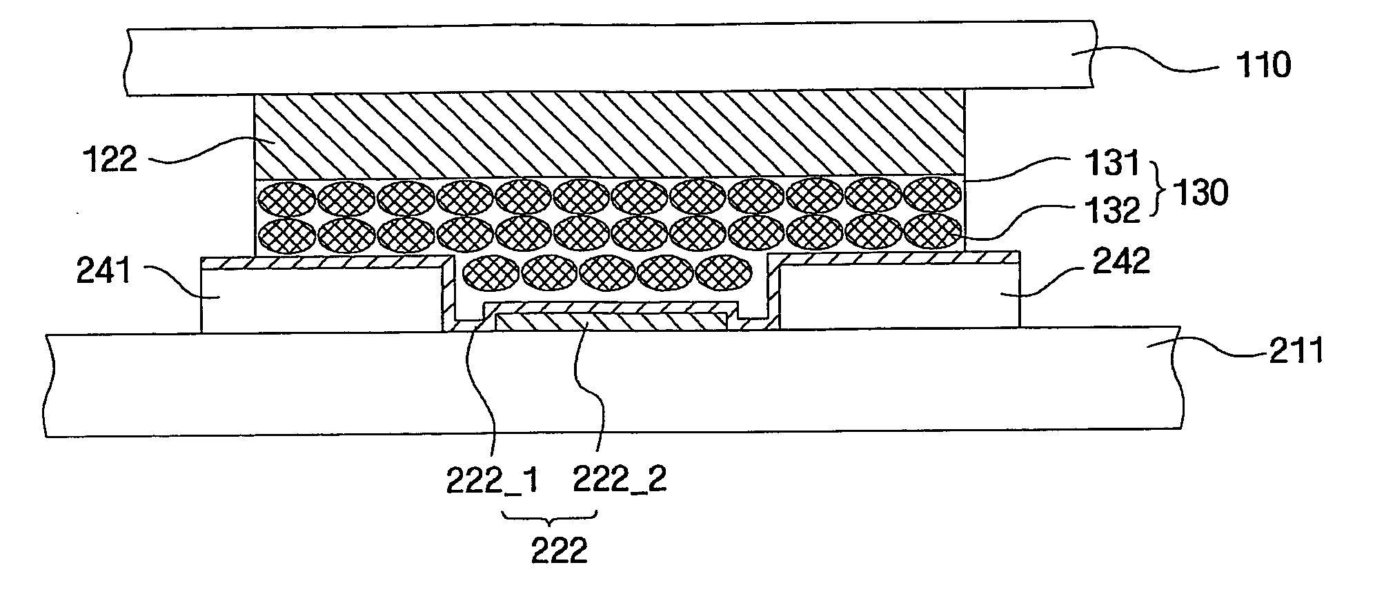
[0030] In a liquid crystal display (LCD) device according to an exemplary embodiment of the present invention, a slit having a length less than that of an overlapping region in which a pad electrode of a liquid crystal panel overlaps with an outer lead of a tape circuit substrate and havin...


PUM


Abstract

A liquid crystal display device includes a liquid crystal panel including a pad electrode, a tape circuit substrate and an anisotropic conductive film. The pad electrode receives one of a driving signal and a power supply voltage signal. The tape circuit substrate includes a base film made of an insulating material, and a signal line formed on the base film and having a slit at a portion of the signal line which overlaps the pad electrode of the liquid crystal panel. The anisotropic conductive film connects the outer lead with the pad electrode.

Description

[0001] This application claims priority from Korean Patent Application No. 10-2004-066274 filed on Aug. 23, 2004 in the Korean Intellectual Property Office, the disclosure of which is incorporated herein by reference in its entirety. BACKGROUND OF THE INVENTION [0002] 1. Field of the Invention [0003] The present invention relates to a tape circuit substrate, a semiconductor chip package including the same, and a liquid crystal display (LCD) device including the semiconductor chip package. More particularly, the present invention relates to a tape circuit substrate capable of improving contact reliability and reducing contact resistance between an outer lead of the tape circuit substrate and a pad electrode of an LCD device, a semiconductor chip package including the tape circuit substrate, and an LCD device including the semiconductor chip package. [0004] 2. Description of the Related Art [0005] There is currently a trend toward production of large sized image display devices, such ...

Claims


Application Information

Patent Timeline
IPC IPC(8): H01L23/495
CPCG02F1/13452H05K1/117H05K3/323H05K3/361H01L2924/0002H05K2201/09663H01L2924/00G02F1/1345
Inventor PARK, HEE-BUMKIM, OCK-JINPARK, JIN-HOLEE, KWANG-SOO
Owner SAMSUNG DISPLAY CO LTD
Why Eureka
Try Eureka