
Dielectric filter

Inactive Publication Date: 2006-02-23
COLLABO INNOVATIONS INC
View PDF7 Cites 18 Cited by
  • Summary
  • Abstract
  • Description
  • Claims
  • Application Information

AI Technical Summary

Benefits of technology

[0015] The present invention is devised to solve the conventional problem. An object of the present invention is to provide a dielectric filter which prevents Q degradation of an inductor and achieves miniaturization without increasing a filter insertion loss.

Problems solved by technology

Considering this restriction, it is not possible to reduce the dielectric filter without degrading its characteristics.

Method used


Image

  • Dielectric filter
  • Dielectric filter
  • Dielectric filter

Examples


embodiment 1

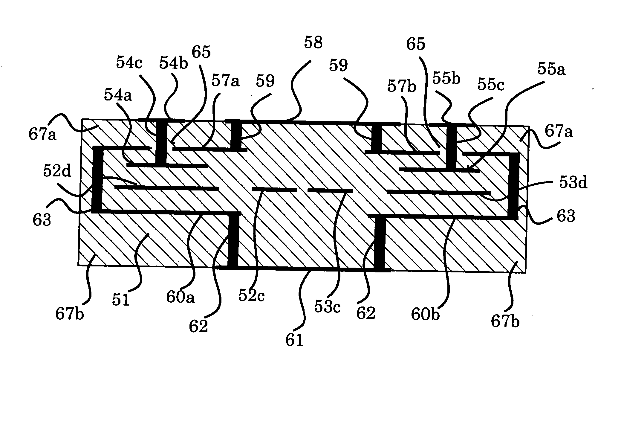
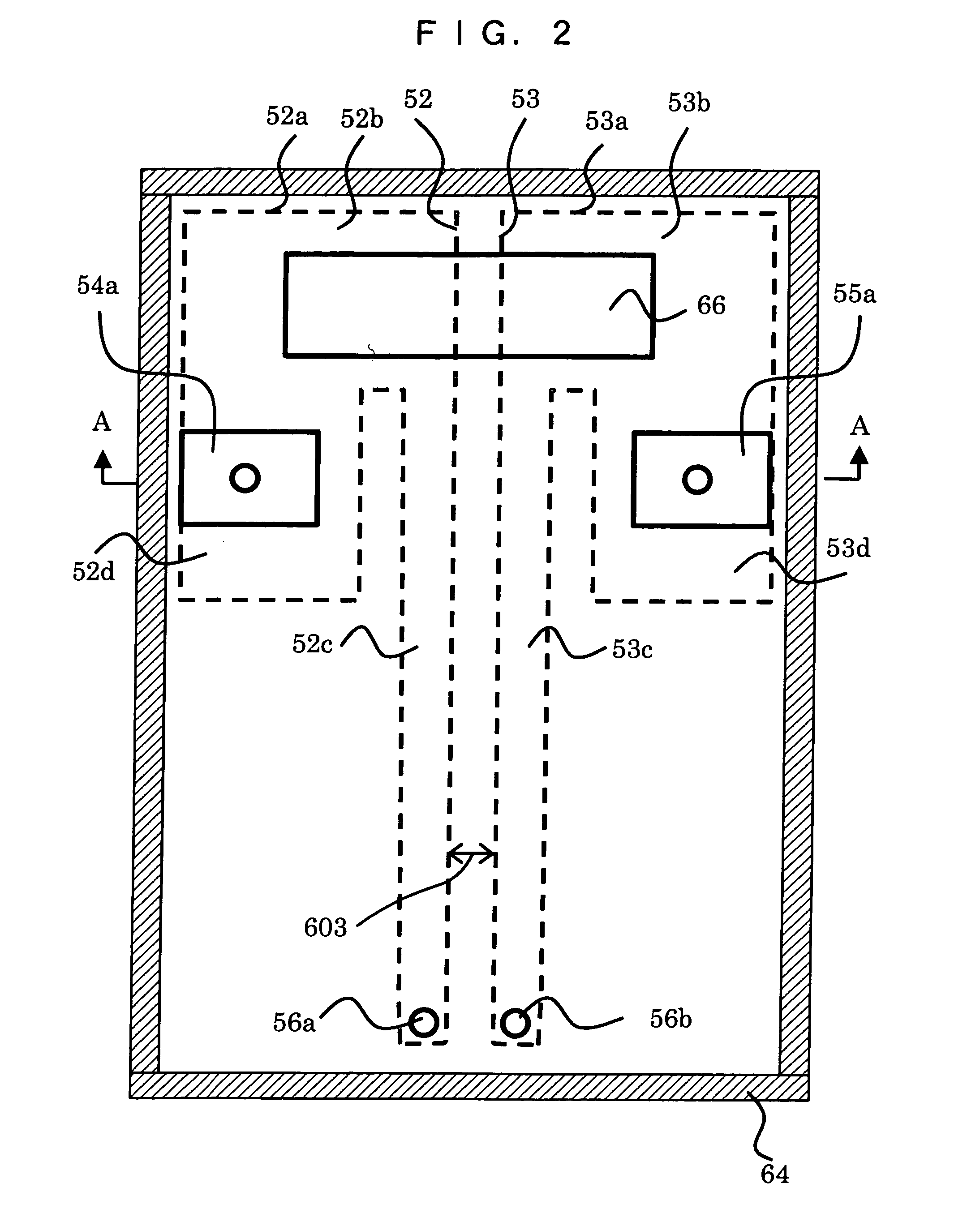
[0054] As shown in FIGS. 1 and 2, a dielectric filter of Embodiment 1 is constituted of first and second resonant elements 52 and 53 each of which is formed in the inner layer of a dielectric substrate 51 and has one open end and the other end connected to the ground via inner vias 56a and 56b, wide portions 52b and 53b which electromagnetically couple the first and second resonant elements 52 and 53 and are formed on the sides of open ends 52a and 53a, narrow portions 52c and 53c formed on the side of a side electrode (a common ground terminal, i.e., the ground) 64 of the first and second resonant elements 52 and 53, bent portions 52d and 53d bent like letter L from the ends of the wide portions 52b and 53b to the side electrode 64, first and second input / output electrodes 54a and 55a formed in the upper layer of the bent portions 52d and 53d, input / output terminals 54b and 55b drawn from the input / output electrodes 54a and 55a, a capacitive electrode 66 formed in the upper layer o...

embodiment 2

[0077]FIG. 8 is a plan view showing a dielectric filter according to Embodiment 2.FIG. 10 is a sectional view taken along line A-A of FIG. 8. FIG. 11 is a sectional view taken along line B-B of FIG. 8. FIG. 12 is an equivalent circuit diagram of FIG. 8. The same constituent elements as Embodiment 1 will be indicated by the same reference numerals and the explanation thereof is simplified.

[0078] Embodiment 2 is different from Embodiment 1 in that two capacitive electrodes 91 and 92 are provided and one ends of the electrodes are directly connected to resonant elements 52 and 53 via inner vias 91a and 92a, respectively. In FIGS. 8, 10, and 11, the capacitive electrode 91 is disposed in the upper layer of a wide portion 53b so as to face a wide portion 52b. The capacitive electrode 91 is directly connected, on the side of the wide portion 53b, to the wide portion 53b via the inner via 91a. Further, the capacitive electrode 92 is disposed in the lower layer of the wide portion 52b so a...

embodiment 3

[0088]FIG. 13 is a sectional view showing a dielectric filter according to Embodiment 3. The dielectric filter of Embodiment 3 is different from Embodiments 1 and 2 in that a ground electrode 166 is provided between input / output electrodes 157a and 158a as shown in FIG. 14. Thus, in the present embodiment, isolation improves between the input / output electrodes 157a and 158a. Further, in the present embodiment, narrow portions 160c and 161c are bent and miniaturized.

[0089] To be specific, as shown in FIG. 13, the dielectric filter of the present embodiment is constituted of a ground electrode 153 provided in a first layer 152 of a dielectric substrate 151, a resonator electrode 155 which is stacked above the ground electrode 153 and provided in a second layer 154, input / output electrodes 157a and 158a which are stacked above the resonator electrode 155 and provided in a third layer 156, and a ground electrode 159 which is stacked above the input / output electrodes 157a and 158a and p...


PUM


Abstract

In order to achieve miniaturization without degrading Q of a dielectric filter in the present invention, resonant elements has upper and lower ground electrodes. The upper ground electrode is formed of upper ground electrodes which correspond to wide portions and have no pattern formed on a portion corresponding to narrow portions, and an upper ground electrode which corresponds to the narrow portions and formed higher than the layer of the upper ground electrodes. The lower ground electrode is formed of lower ground electrodes which correspond to the wide portions and have no pattern formed on a portion corresponding to the narrow portions, and a lower ground electrode which corresponds to the narrow portions and formed lower than the layer of the ground electrodes.

Description

FIELD OF THE INVENTION [0001] The present invention relates to a dielectric filter used for a high frequency apparatus and the like. BACKGROUND OF THE INVENTION [0002] A conventional dielectric filter will be described below. FIG. 21 is a plan view showing the conventional dielectric filter. FIG. 22 is a sectional view taken along line A-A of FIG. 21. [0003] The dielectric filter is constituted of first and second resonant elements 2 and 3 each of which is formed in the inner layer of a dielectric substrate 1 and has one open end and the other end connected to the ground, wide portions 2b and 3b which electromagnetically couple the first and second resonant elements 2 and 3 with each other and are formed on the sides of open ends 2a and 3a, narrow portions 2c and 3c formed on the side of a side electrode (a common ground terminal, i.e., the ground) 12 of the first and second resonant elements 2 and 3, bent portions 2d and 3d bent like letter L from the ends of the wide portions 2b a...

Claims


Application Information

Patent Timeline
IPC IPC(8): H01P1/203
CPCH01P1/20345
Inventor SHINABE, MUNEHIRO
Owner COLLABO INNOVATIONS INC
Features
  • Generate Ideas
  • Intellectual Property
  • Life Sciences
  • Materials
  • Tech Scout
  • Unparalleled Data Quality
  • Higher Quality Content
  • 60% Fewer Hallucinations
Learn More