

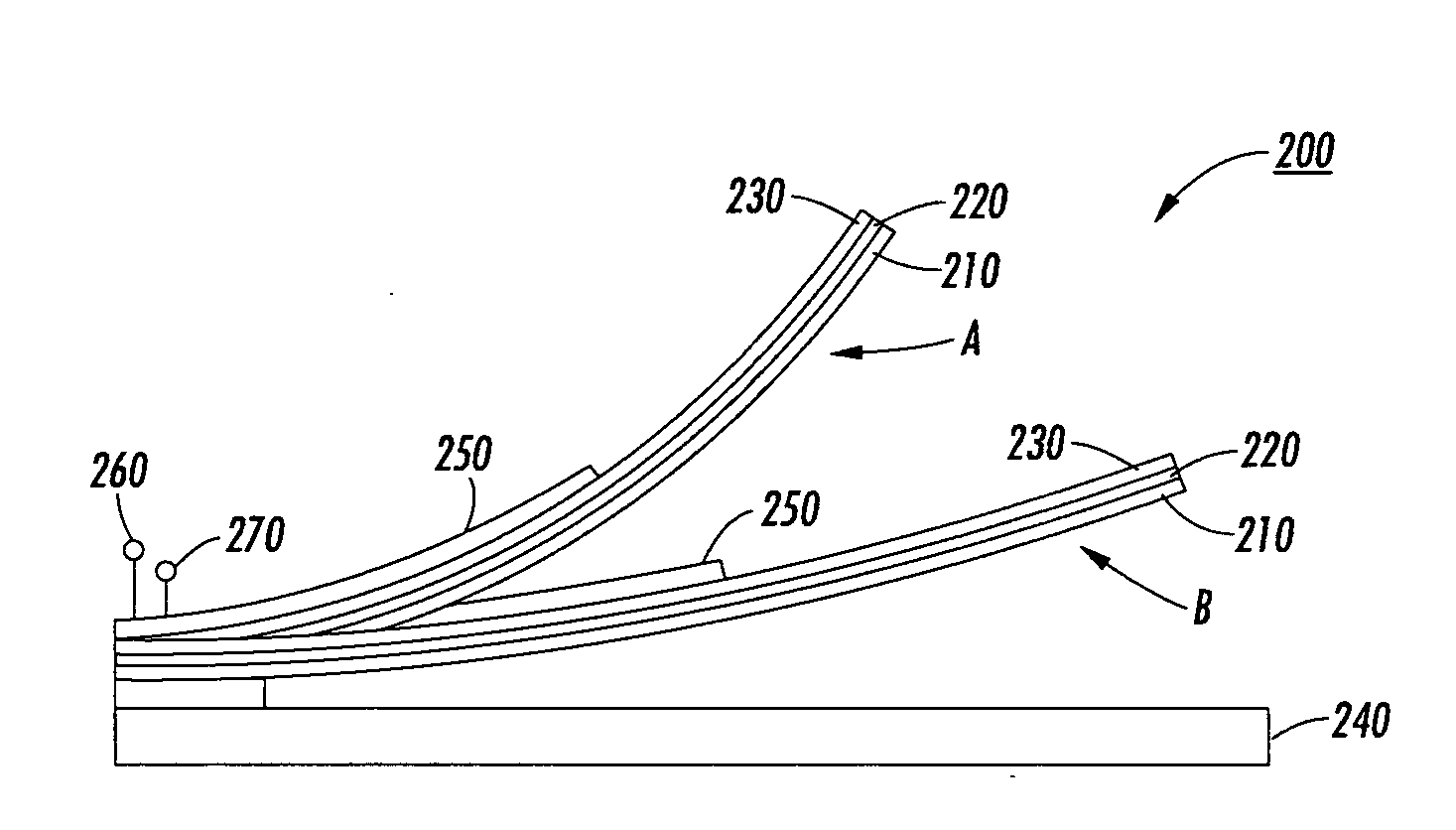
Stressed material and shape memory material MEMS devices and methods for manufacturing
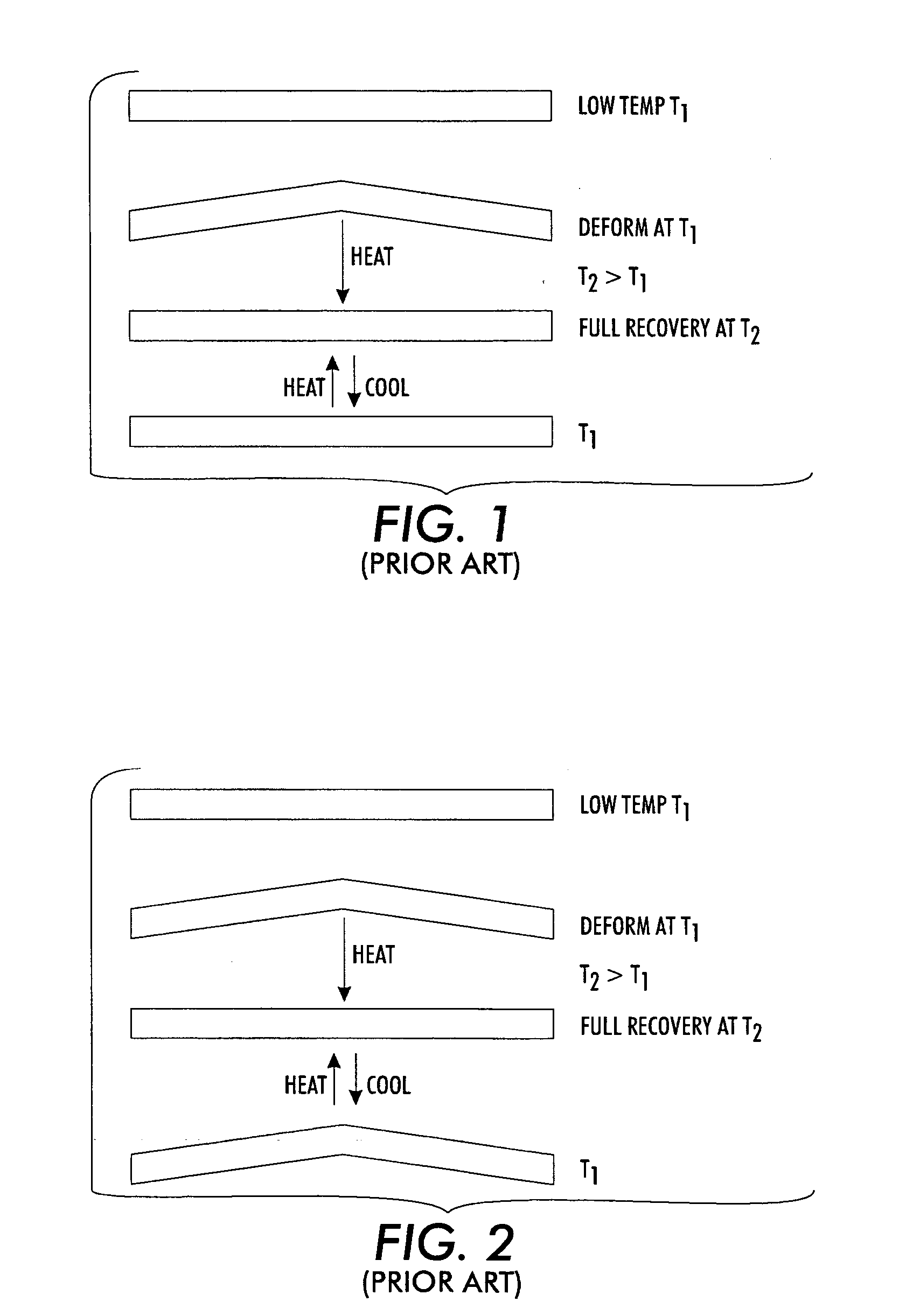
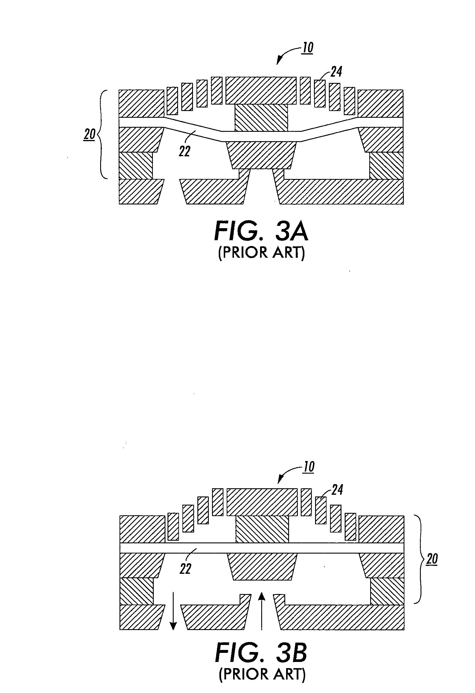
a stress-based material and shape-based technology, applied in the field of stress-based material and shape-based shape-based material mems devices and manufacturing methods, can solve the problems of plastic deformation in the material, the size of the resulting mems devices is also unsatisfactory, and the un-deformed state is retained
- Summary
- Abstract
- Description
- Claims
- Application Information
AI Technical Summary
Problems solved by technology
Method used
Image

Examples
example 1
Stressed Metal (MoCr) / SMA (TiNi) Film Actuator Model
[0091] An actuator was modeled having a length of 500 μm, a thickness of 3.75 μm, and a width of 100 μm. The actuator included a 1.75 μm-thick TiNi layer, a 1 μm thick MoCr layer with −1 GPa deposited compressive stress, and a 1 μm thick MoCr layer with +1 GPa deposited tensile stress. Tip displacement (μm) and spring constant (N / m) of the actuator are calculated and tabulated in Table 1, below.
example 2
Piezoelectric PZT Bimorph Actuator Model
[0092] An actuator also having a length of 500 μm, a thickness of 3.75 μm, and a width of 100 μm was modeled. The structure of the actuator included of two PZT films, each of which was 1.875 μm thick. Tip displacement (μm) and spring constant (N / m) of the actuator are calculated and tabulated in Table 1.
example 3
Si / Al Thermal Actuator Model
[0093] An actuator also having a length of 500 μm, a thickness of 3.75 μm, and a width of 100 μm was modeled. The structure of the actuator included a 1.5 μm thick Si film and 2.25 μm-thick Al film. Tip displacement (μm) and spring constant (N / m) of the actuator are calculated and tabulated in Table 1.
PUM
 Abstract
Description
Claims
Application Information