Semiconductor device, method and apparatus for testing same, and method for manufacturing semiconductor device

Active Publication Date: 2006-03-02
RENESAS ELECTRONICS CORP
View PDF6 Cites 14 Cited by
  • Summary
  • Abstract
  • Description
  • Claims
  • Application Information

AI Technical Summary

Benefits of technology

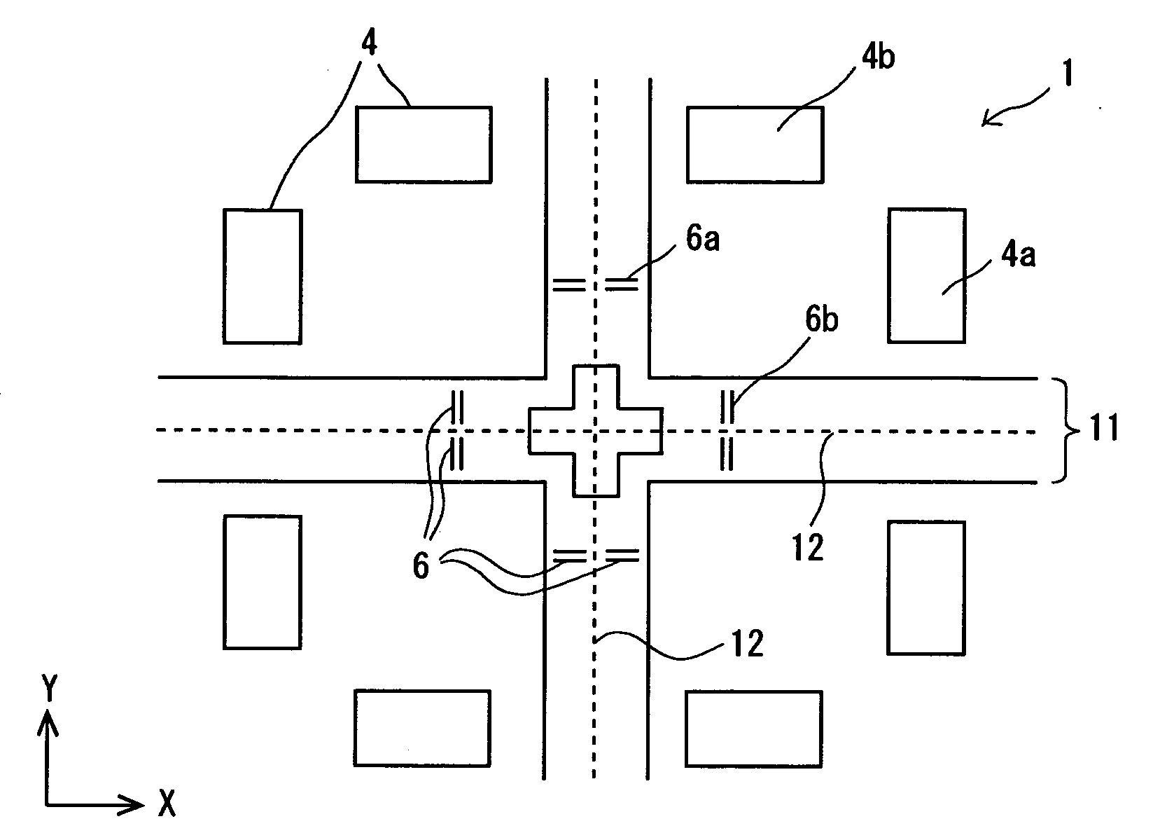
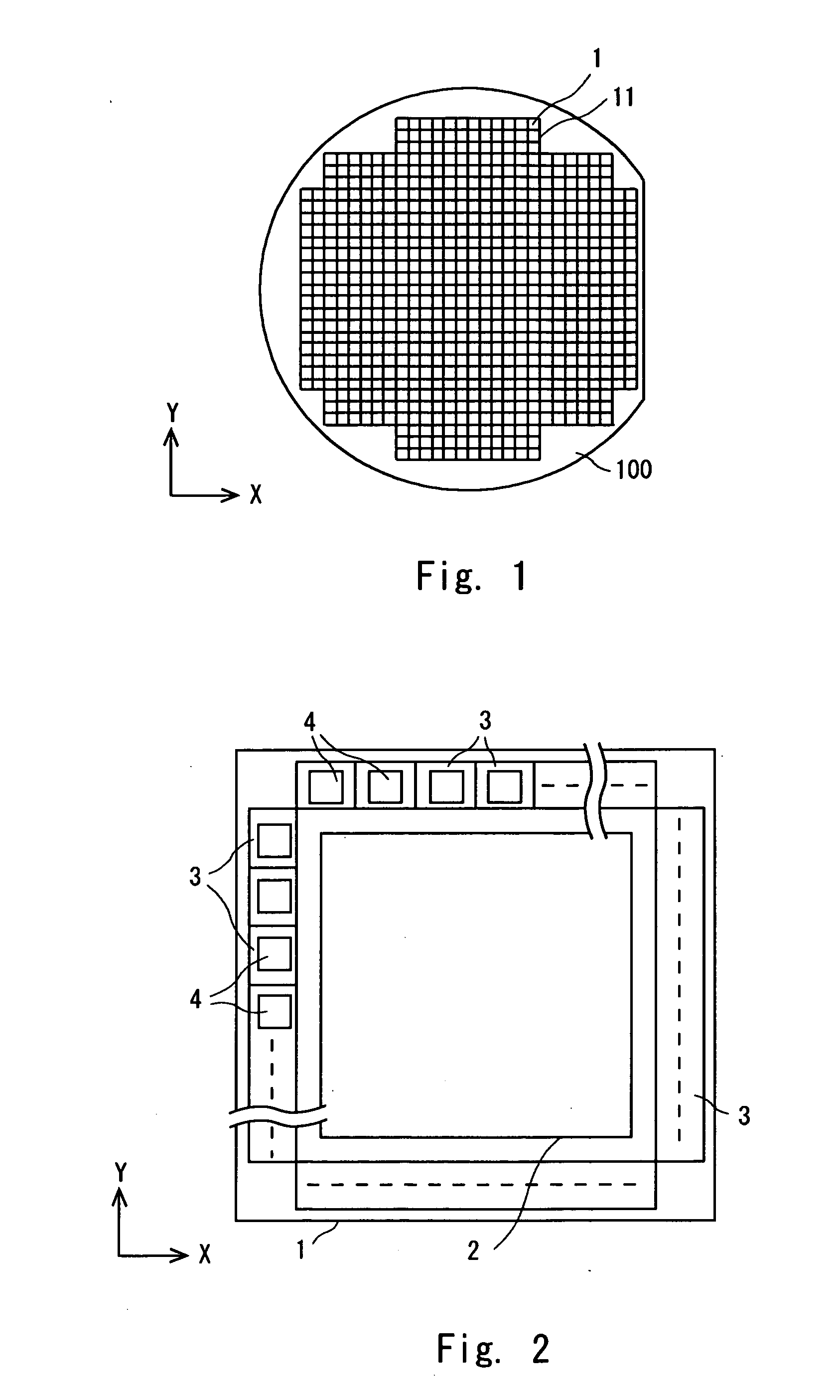
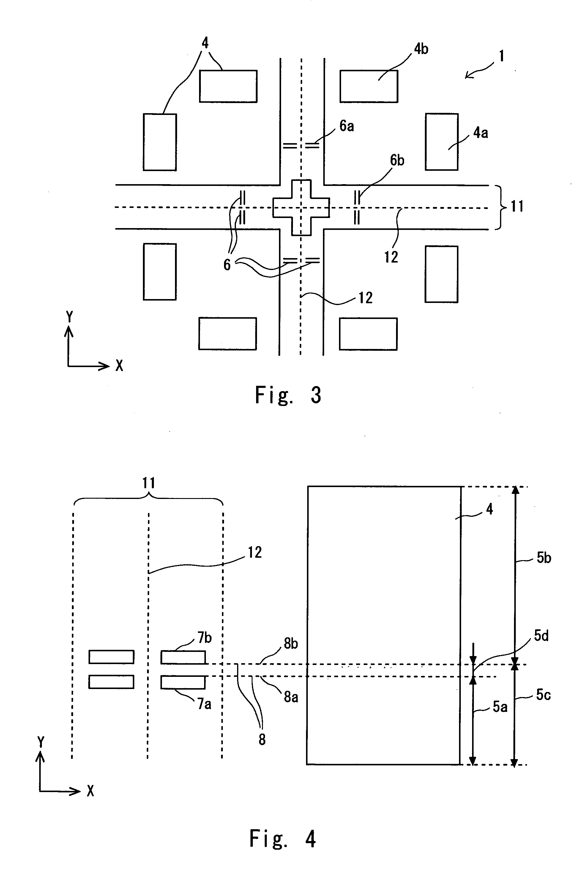
[0011] According to one aspect of the invention, there is provided a semiconductor device, which includes a probe area mark for defining a probe area for contacting a test probe to an electrode pad, wherein the probe area mark is disposed away from the electrode pad. By means of the semiconductor device of the present invention, a probe area (mark) can be recognized reliably, and testing can be conducted accurately.
[0012] According to another aspect of the invention, there is provided a semiconductor device, which includes an electrode pad to be contacted a test probe for performing probe testing, a bonding area mark for defining a bonding area which performs wire boding on the electrode pad, and a probe area mark for defining a probe repair area for repairing or replacing the test probe for the electrode pad. By means of the semiconductor device, occurrence of defective products can be prevented, and productivity can be improved.
[0013] According to still another aspect of the invention, there is provided a testing method of the semiconductor device, contacting a test probe to an electrode pad provided in a semiconductor device to perform electrical testing on the semiconductor device, which includes recognizing a probe area mark provided away from the electrode pad, and determining the position of the test probe to a probe area which is defined by the probe area mark. By means of the testing method of the present invention, positioning can be performed accurately, and also accurate testing can be conducted.
[0014] According to yet another aspect of the invention, there is provided a testing method of a semiconductor device, comprising, which is includes contacting a test probe to an electrode pad provided in a semiconductor device to perform electrical testing on the semiconductor device, determining whether or not probe damage of the test probe provided in the electrode pad is present in a probe repair area, repairing or replacing the test probe when it is determined that the probe damage is present in the probe repair area, determining, for the electrode pad in which determination is made that the probe damage is present in the probe repair area, whether or not the probe damage is present in a bonding area and judging that the semiconductor device, which has the electrode pad in which the determination is made that the probe damage is present in the bonding area, as a defective product. By means of the testing method, a test probe can be repaired or replaced before defective products are produced, thus occurrence of defective products can be minimized.
[0015] According to still another aspect of the invention, there is provided a testing apparatus of a semiconductor device, which includes a probe test execution portion which contacts a test probe to an electrode pad provided in the semiconductor device to perform electrical testing of the semiconductor device, a probe repair determination portion which determines whether or not probe damage of the test probe, which is formed on the electrode pad, is present in a probe repair area, and a defective product determination portion which, for an electrode pad in which determination is made that the probe damage is present in the probe repair area, determines whether the semiconductor device is a defective product or not based on whether or not the probe damage is present in a bonding area. By means of the testing apparatus of the present invention, a test probe can be repaired or replaced before defective products are produced, thus occurrence of defective products can be minimized.
[0016] According to yet another aspect of the invention, there is provided a method for manufacturing a semiconductor device, which includes contacting a test probe to an electrode pad provided in a semiconductor device to perform electrical testing of the semiconductor device, repairing or replacing the test probe based on whether or not probe damage of the test probe provided in the electrode pad is present in a probe repair area, judging whether the semiconductor device is a non-defective product or defective product based on whether or not the probe damage is present in a bonding area in the electrode pad in which determination is made that the probe damage is present in the probe repair area, and bonding an external electrode to the bonding area of the electrode pad for the semiconductor device which is judged as a non-defective product. By means of the manufacturing method of the present invention, a test probe can be repaired or replaced before defective products are produced, thus productivity can be improved.

Problems solved by technology

In such a semiconductor device, when bringing a test probe into contact with the surface of an electrode pad when performing probing, a contact damage called “probe damage” is generated on the surface of the electrode pad.
Therefore, the problem was that reliability of bonding is decreased.
Particularly, a problem is generated when connecting an aluminum electrode pad with gold wire by ultrasonic bonding, because this bonding is performed by forming an alloy of aluminum and gold on the surface of the electrode pad, so the bonded surface is decreased due to the probe damage, whereby the bonding strength between the gold wire and electrode pad is decreased.
However, there are the following problems in the conventional testing.
In this case, the electrode pad is an obstacle to realizing high scale integration of the semiconductor.
Particularly, with the recent multifunction of a semiconductor, the number of electrode pads is increasing, so it is difficult to achieve a multifunctional and highly integrated semiconductor device.
Specifically, location accuracy at the time when the probe is brought into contact with the electrode pad formed on the surface of the wafer is decreased due to deterioration of the physical strength of the probe.
In this case, after testing is executed in the state where the probe is deteriorated, the probe damage is detected in a detection process.
Therefore, there occur problems that yield cannot be improved, and that it is difficult to improve productivity.
Hence, It has now been discovered that testing cannot be performed accurately with the conventional testing method of a semiconductor device, whereby it is difficult to improve productivity.

Method used


Image

  • Semiconductor device, method and apparatus for testing same, and method for manufacturing semiconductor device
  • Semiconductor device, method and apparatus for testing same, and method for manufacturing semiconductor device
  • Semiconductor device, method and apparatus for testing same, and method for manufacturing semiconductor device

Examples


Embodiment Construction

[0027] The invention will be now described herein with reference to illustrative embodiments. Those skilled in the art will recognize that many alternative embodiments can be accomplished using the teachings of the present invention and that the invention is not limited to the embodiments illustrated for explanatory purposed.

[0028] The configuration of the semiconductor device related to the present invention is explained hereinafter. The semiconductor device in accordance with one aspect of the present invention has an electrode pad to be contacted a test probe accurately. Further, the semiconductor device has a probe area mark. The probe area mark defines a probe area for contacting a test probe to the electrode pad. Preferably, the probe area mark is disposed away from the electrode pad. The semiconductor device in accordance with another aspect of the present invention has the electrode pad to be contacted a test probe for performing probe testing. Further, the semiconductor de...


PUM


Abstract

The semiconductor device according to an aspect of the present invention is a semiconductor device having an electrode pad to be contacted a test probe for performing probe testing, a bonding area mark for defining a bonding area which performs wire boding on the electrode pad, and a probe area mark for defining a probe repair area for repairing or replacing the test probe for the electrode pad.

Description

BACKGROUND OF THE INVENTION [0001] 1. Field of the Invention [0002] The present invention relates to a semiconductor device comprising an electrode pad for external connection (referred to as “electrode pad” hereinafter), a method and apparatus for testing the semiconductor device, and a method for manufacturing the semiconductor device. Particularly the invention relates to a semiconductor device comprising an electrode pad which contacts a test probe for electrical characteristic testing, a method and apparatus for testing the semiconductor device, and a method for manufacturing the semiconductor device. [0003] 2. Description of the Related Art [0004] In a semiconductor device in the form of a chip, which is formed on a semiconductor substrate, electrical characteristic testing is performed by bringing a test probe of an electrical characteristic testing apparatus into contact with an electrode pad provided in the semiconductor device, which is so called “probing”, before mounting...

Claims


Application Information

Patent Timeline
IPC IPC(8): G01R31/02
CPCG01R31/2884H01L2224/05554H01L24/06H01L2224/02166H01L2224/0401H01L2224/05553H01L2224/05624H01L2224/45144H01L2924/01002H01L2924/01004H01L2924/01005H01L2924/01013H01L2924/01014H01L2924/01033H01L2924/01079H01L2924/01082H01L2924/014H01L24/03H01L2924/01006H01L2224/48624H01L2924/00H01L22/32H01L22/00
Inventor JIMI, JUNICHI
Owner RENESAS ELECTRONICS CORP
Why Eureka
Try Eureka