Selecting adjustment for OLED drive voltage

Inactive Publication Date: 2006-03-02
EASTMAN KODAK CO
View PDF6 Cites 123 Cited by
  • Summary
  • Abstract
  • Description
  • Claims
  • Application Information

AI Technical Summary

Benefits of technology

[0010] It is an advantage of this invention that it provides for a lower power consumption of an OLED device.
[0011] It is another advantage of this invention that it can provide for an increased lifetime for an OLED device.
[0012]

Problems solved by technology

A problem with existing OLED devices is that of power consumption.
Because of inherent manuf

Method used


Image

  • Selecting adjustment for OLED drive voltage
  • Selecting adjustment for OLED drive voltage
  • Selecting adjustment for OLED drive voltage

Examples


Embodiment Construction

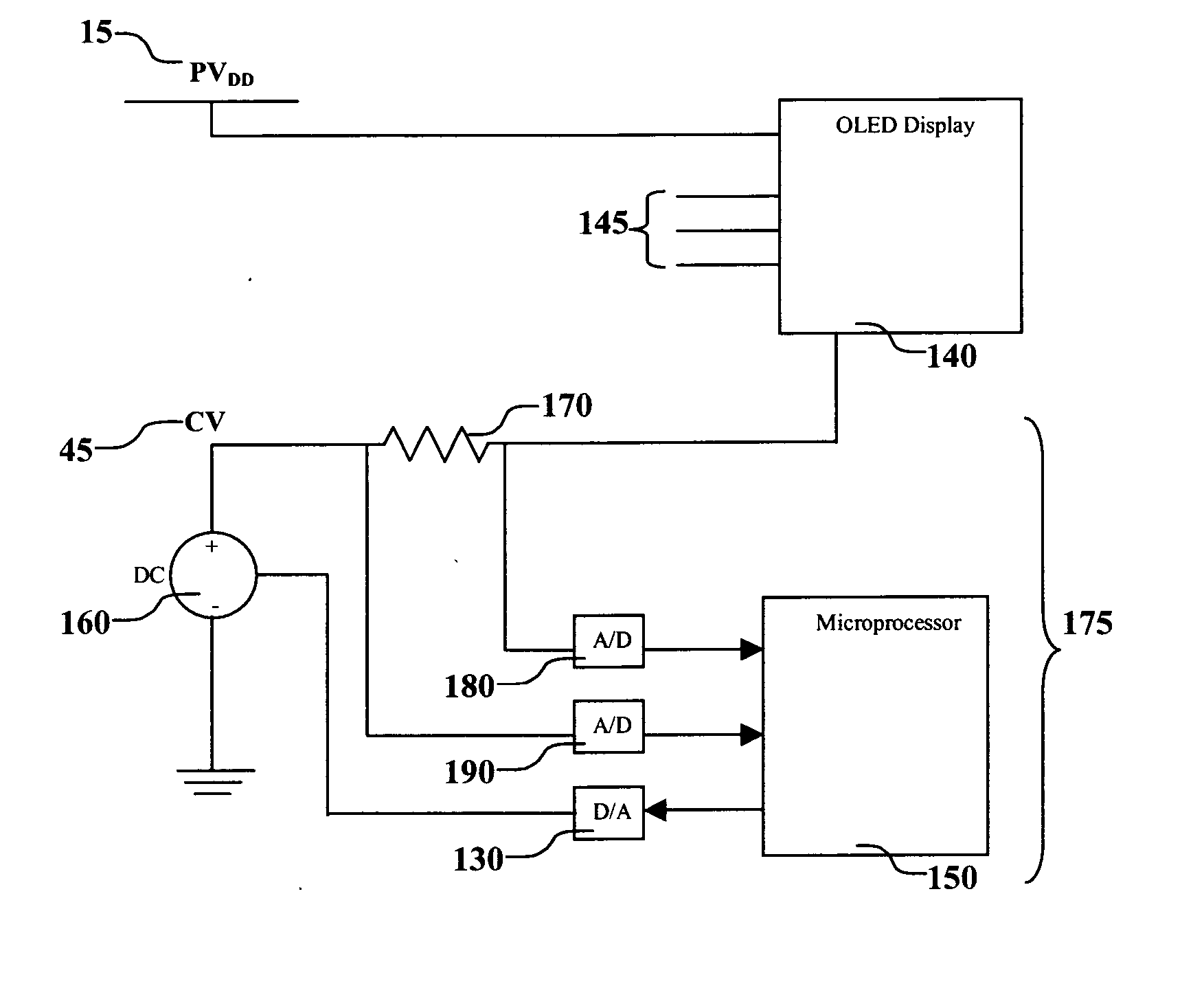
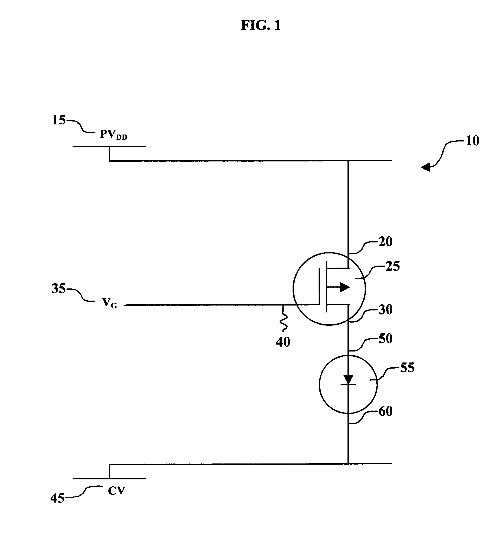
[0023]FIG. 1 shows a schematic of one embodiment of the basic circuitry of an OLED pixel of an active matrix display. OLED circuit 10 includes a p-type thin-film transistor 25 and the organic layers 55 of an OLED device. Organic layers 55 include a light-emitting layer, and can also include a hole-transporting layer, an electron-transporting layer, and other layers known to be useful in an OLED device. The materials comprising organic layers 55 have been described in detail in U.S. Pat. No. 6,555,284 by Boroson et al. The circuit includes three voltages: power voltage (PVDD) 15 that is connected to the source 20 of transistor 25; gate voltage (VG) 35 that is connected to gate 40 of transistor 25; and cathode voltage (CV) 45 that is connected to the cathode 60 of the organic layers 55. Drain 30 of transistor 25 is connected to anode 50 of organic layers 55. The difference between power voltage 15 and cathode voltage 45 (PVDD−CV) is the drive voltage for the device. Gate voltage 35 re...


PUM


Abstract

A method for selecting an adjustment for at least one drive voltage used to drive an OLED display to reduce power consumption including operating the display to produce a calibration curve which depicts the drive voltage versus current or luminance, and selecting the adjustment for the drive voltage based upon the calibration curve so as to reduce the power consumed by the OLED display while maintaining desired luminance throughout the lifetime of the OLED display.

Description

CROSS REFERENCE TO RELATED APPLICATIONS [0001] Reference is made to commonly assigned U.S. patent application Ser. No. 10 / 767,288 filed Jan. 28, 2004 by Seiichi Mizukoshi et al., entitled “Setting Black Levels in Organic EL Display Devices”, and commonly assigned U.S. patent application Ser. No. 10 / 812,546 filed Mar. 29, 2004 by Seiichi Mizukoshi et al., entitled “Controlling Current in Display Device”, the disclosures of which are herein incorporated by reference.FIELD OF THE INVENTION [0002] The present invention relates to OLED displays and to reducing the power consumption thereof. BACKGROUND OF THE INVENTION [0003] In electroluminescent (EL) displays (also known as organic light-emitting diode devices, or OLED devices) the basic OLED device has in common a spaced anode and cathode, and an organic EL medium sandwiched between the anode and the cathode. The organic EL medium can include of one or more layers of organic thin films, where one of the layers is primarily responsible ...

Claims


Application Information

Patent Timeline
IPC IPC(8): G09G3/30
CPCG09G3/3225G09G2320/0233G09G2320/0285G09G2360/145G09G2320/043G09G2320/0693G09G2330/021G09G2320/029
Inventor HADCOCK, DAVID HAROLD
Owner EASTMAN KODAK CO
Why Eureka
Try Eureka