Methods and systems for purifying elements

a technology of elements and purification methods, applied in the direction of crystal growth process, polycrystalline material growth, silicon compounds, etc., can solve the problem of limited use of such systems by the cost of the semiconductor material in the semiconductor wafers (in particular, silicon) needed for such systems, and the crystalline silicon solar cell industry is quickly running out of cost-effective feedstocks

Inactive Publication Date: 2006-03-09
HERITAGE POWER
View PDF9 Cites 58 Cited by
  • Summary
  • Abstract
  • Description
  • Claims
  • Application Information

AI Technical Summary

Benefits of technology

[0022] a solidifier which can create conditions under which a part of said liquefied material will directionally solidify to convert the liquefied material to a combination of purified solidified material and liquid remainder;
[0023] a liquid remover which can remove the liquid remainder from the container; and
[0024] a second melter which can create conditions under which the purified solidified material melts to form a re-liquefied purified material.
[0026] The present invention thus provides methods and systems for providing silicon feedstock for solar-electric applications more cost effectively than existing methods and systems. The methods and systems of the present invention provide a manufacturing-compatible-processing method to effect purification, including means for continuously removing impurity-laden material.

Problems solved by technology

A significant portion of the cost of such semiconductor material is the semiconductor material itself.
For example, in the case of solar-electric systems, a primary factor which has limited the use of such systems is the cost of the semiconductor material in the semiconductor wafers (in particular, silicon) needed for such systems.
The crystalline silicon solar cell industry is quickly running out of cost-effective feedstock.
The prevailing approach for manufacturing silicon feedstock has been well developed for the semiconductor industry (i.e., production of semiconductor-grade silicon), but does not meet the requirements for the production of large amounts of cheap, moderate purity, solar-grade solid-silicon feedstock.

Method used


Image

  • Methods and systems for purifying elements
  • Methods and systems for purifying elements
  • Methods and systems for purifying elements

Examples


Embodiment Construction

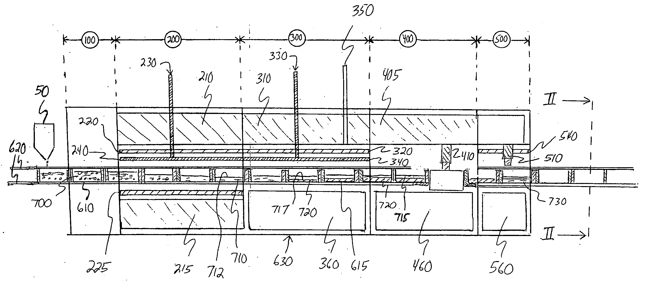
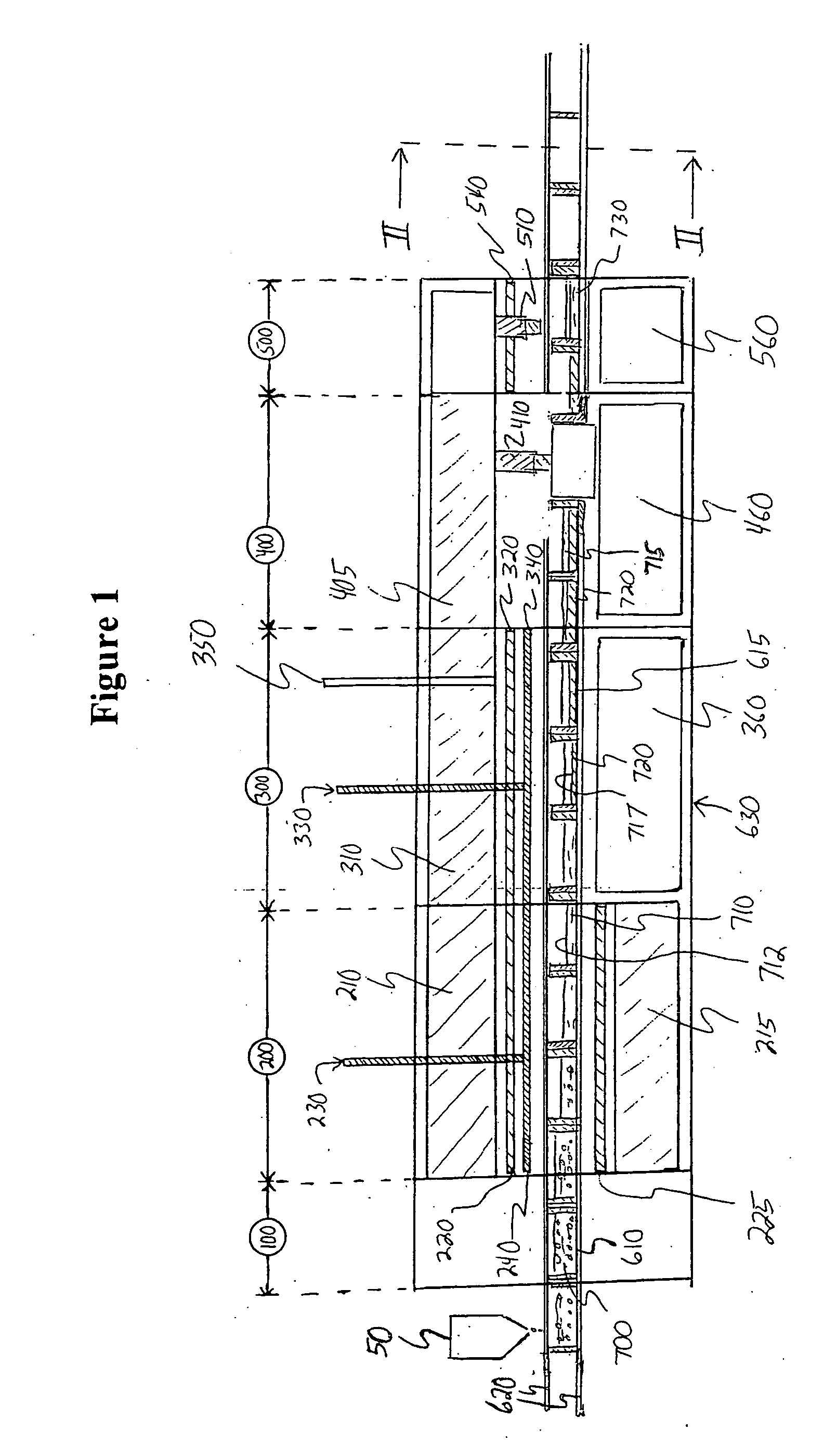
[0030] The raw material treated by the methods according to the present invention and / or supplied to systems according to the present invention is generally any material containing the element or elements being purified, preferably any material which readily exists in a liquid state (e.g., silicon, germanium, aluminum, iron, etc.). For example, in cases where solar-grade silicon is sought, the input can be any silicon-containing material, e.g., metallurgical silicon, recycle scrap silicon, etc. Where solar-grade silicon is sought, one example of a suitable raw material is metallurgical silicon having a purity level of 98 to 99% (major impurities being Al, Fe, Ca, and / or Ti), selected or processed to have concentrations of B and P less than 10 ppmw.

[0031] The raw material is deposited into a container, e.g., a crucible. The raw material may be liquid or solid (or a mixture of liquid and solid) when it is deposited into a container.

[0032] Where the raw material is solid, it is prefe...


PUM

PropertyMeasurementUnit
depthaaaaaaaaaa
sizeaaaaaaaaaa
temperatureaaaaaaaaaa

Abstract

There are provided methods of purifying a material, comprising melting solid material to form liquefied material, directionally solidifying a portion of the liquefied material; and removing a liquid remainder from the purified solidified material. Preferably, the purified solidified material is melted to form re-liquefied purified material, and re-liquefied purified material is removed. Preferably, the material is positioned in a container as it is being purified. The method is particularly useful for purifying elemental material, e.g., semiconductor material such as silicon and / or germanium, such as recycle scrap silicon and / or metallurgical grade silicon. There are also provided systems for carrying out such methods.

Description

CROSS REFERENCE TO RELATED APPLICATION [0001] This application claims the benefit of U.S. Provisional Application Ser. No. 60 / 414,052 filed Sep. 27, 2002, the entirety of which is incorporated herein by reference.FIELD OF THE INVENTION [0002] The present invention relates to methods and systems for purifying elements. In one aspect, the present invention is directed to methods and systems for purifying semiconductor elements, e.g., silicon and germanium. In a specific aspect, the present invention relates to purification of metallurgical-grade silicon and / or scrap silicon into solar-grade silicon. BACKGROUND OF THE INVENTION [0003] Purified elemental material is used for a variety of purposes. For instance, purified semiconductor elemental material is needed for a variety of applications, and there is an ever-increasing demand for such material in most, if not all, of such applications. [0004] Currently, silicon is the most commonly used semiconductor material, e.g., for making semi...

Claims


Application Information

Patent Timeline
Patent Type & Authority Applications(United States)
IPC IPC(8): C30B13/00C30B19/00C01B33/02C01B33/039H01L
CPCC01B33/037C01B33/039C30B29/06C30B13/00C30B15/00C30B11/00
Inventor HALL, ROBERT B.KENDALL, SCOTT L.RAND, JAMES A.SIMS, PAUL E.
Owner HERITAGE POWER
Why Eureka
Try Eureka