
Thin module system and method

a technology of thin modules and modules, applied in the direction of printed circuit aspects, electrical apparatus construction details, instruments, etc., can solve the problems of limited profile space for such devices, come with some cost, eventually be self-limiting, etc., and achieve the effect of reducing profiles

Active Publication Date: 2006-03-09
TAMIRAS PER PTE LTD LLC
View PDF99 Cites 82 Cited by
  • Summary
  • Abstract
  • Description
  • Claims
  • Application Information

AI Technical Summary

Benefits of technology

[0012] Modules with more area for device mounting but minimized profiles are provided. In preferred embodiments, modules that employ one or more flex circuits have sculpted supportive substrates to selectively accomm

Problems solved by technology

Systems that employ DIMMs provide, however, very limited profile space for such devices and conventional DIMM-based solutions have typically provided only a moderate amount of memory expansion.
This improvement has, however, come with some cost and will eventually be self-limiting.
Another coming issue in memory module strategy and design arises from expected increases in circuit die sizes and the concomitant increases in package sizing.
When packaged, it is expected that typical DRAMs of coming densities and capacities will not readily fit on 30 mm.
Consequently, conventional DIMM design is unlikely to accommodate the underlying memory technology as die sizes rise to meet the ubiquitous pressures for greater capability.
The additional connection may cause, however, flawed signal integrity for the data signals passing from the DIMM to the daughter card and the additional thickness of the daughter card(s) increases the profile of the DIMM.
Further, the MDP scheme may exhibit increased costs because of increased yield loss from packaging together multiple die that are not fully pre-tested.
The increased component height of some stacking techniques may alter, however, system requirements such as, for example, required cooling airflow or the minimum spacing around a circuit board on its host system.

Method used


Image

  • Thin module system and method
  • Thin module system and method
  • Thin module system and method

Examples


Embodiment Construction

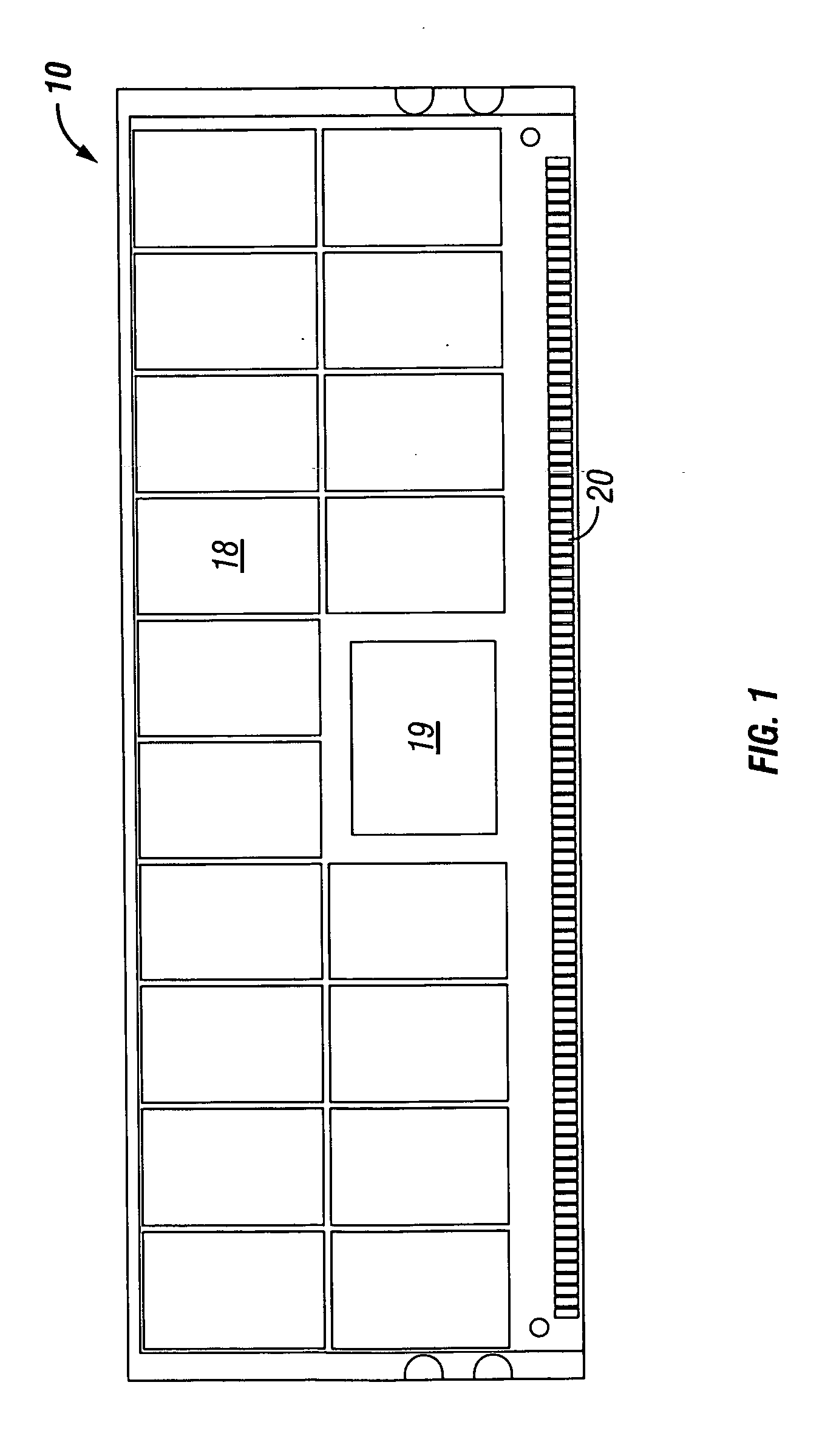
[0036]FIG. 1 depicts a preferred embodiment devised in accordance with the present invention. Module 10 is depicted in FIG. 1 exhibiting ICs 18 and circuit 19.

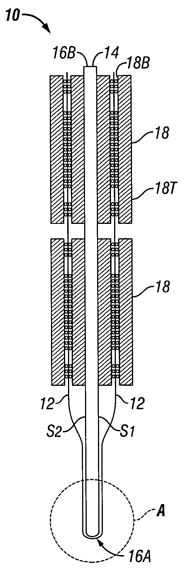
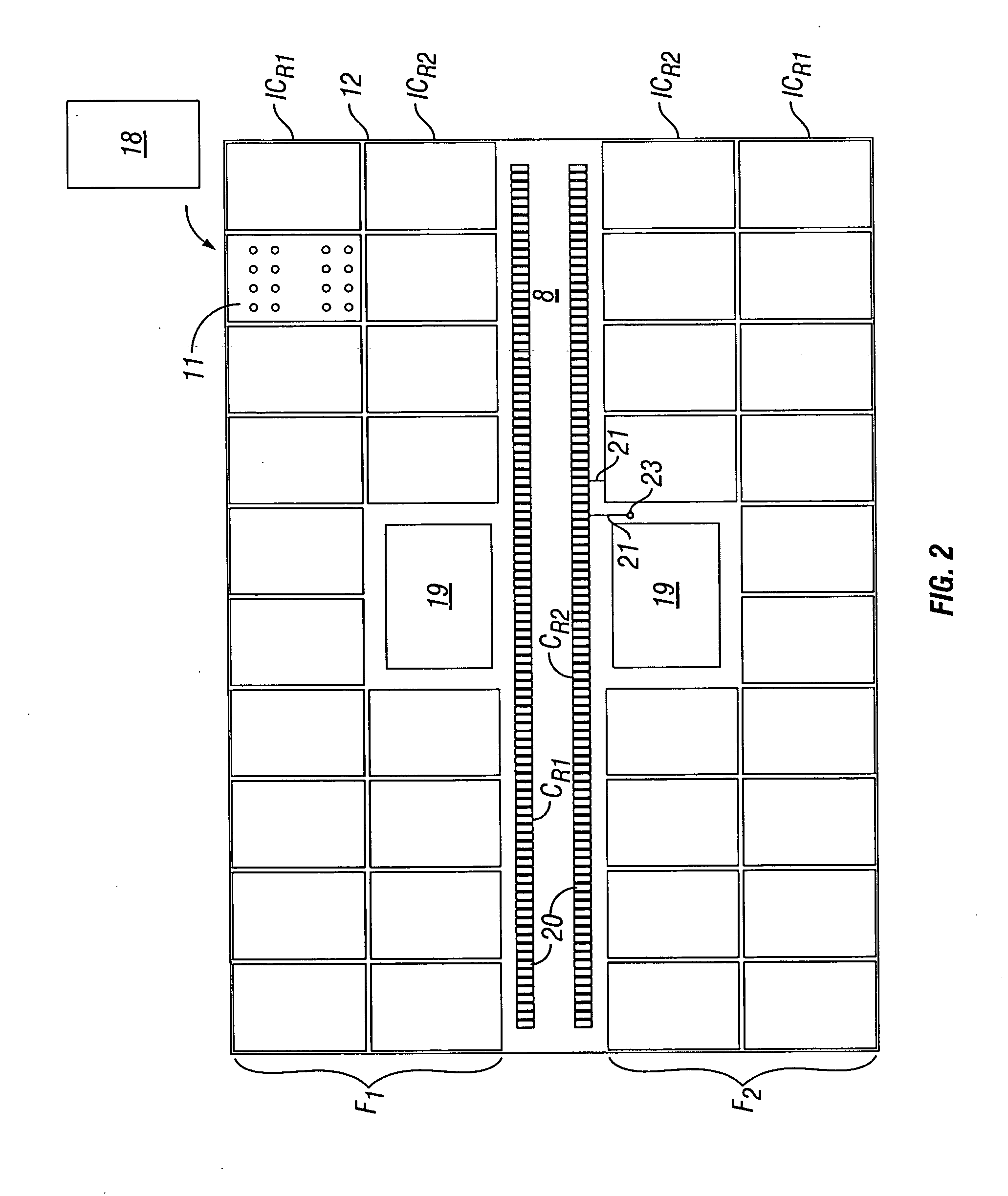
[0037]FIG. 2 depicts a first side 8 of flex circuit 12 (“flex”, “flex circuitry”, “flexible circuit”) used in constructing a module according to an embodiment of the present invention. Flex circuit 12 is preferably made from one or more conductive layers supported by one or more flexible substrate layers as further described with reference to later Figs. The construction of flex circuitry is known in the art. The entirety of the flex circuit 12 may be flexible or, as those of skill in the art will recognize, the flexible circuit structure 12 may be made flexible in certain areas to allow conformability to required shapes or bends, and rigid in other areas to provide rigid and planar mounting surfaces. Preferred flex circuit 12 has openings 17 for use in aligning flex circuit 12 to substrate 14 during assembly.

[0038] ICs 18 o...


PUM


Abstract

Modules with larger areas for device mounting but minimized profiles are provided. In preferred embodiments, modules that employ one or more flex circuits have sculpted supportive substrates to selectively accommodate larger or taller profile devices. In several preferred embodiments, higher profile circuits such as AMBs, for example, are disposed in what are, in a preferred embodiment, windows, pockets, or cutaway areas in the substrate. In other preferred embodiments, both the substrate and the flexible circuitry have openings into which a device of greater profile such as, for example, an AMB or a logic device with or without a resident heat sink are provided with a volume to occupy without adding the full profile of the taller device to the profile of the module itself.

Description

RELATED APPLICATIONS [0001] This application is a continuation-in-part of U.S. patent application Ser. No. 11 / 007,551, filed Dec. 8, 2004 and a continuation-in-part of U.S. patent application Ser. No. 11 / 005,992, filed Dec. 7, 2004 both of which are, in turn, continuations-in-part of U.S. patent application Ser. No. 10 / 934,027, filed Sep. 3, 2004. U.S. patent application Ser. No. 11 / 007,551, U.S. patent application Ser. Nos. 11 / 005,992 and 10 / 934,027 are each incorporated by reference herein.TECHNICAL FIELD [0002] The present invention relates to systems and methods for creating high density circuit modules. BACKGROUND OF THE INVENTION [0003] The well-known DIMM (Dual In-line Memory Module) board has been used for years, in various forms, to provide memory expansion. A typical DIMM includes a conventional PCB (printed circuit board) with memory devices and supporting digital logic devices mounted on both sides. The DIMM is typically mounted in the host computer system by inserting a...

Claims


Application Information

Patent Timeline
IPC IPC(8): H01L23/02
CPCG11C5/04H05K1/0203H05K1/118H05K1/181H05K1/189H05K2203/1572H05K2201/056H05K2201/1056H05K2201/10734H05K2201/2018H05K3/0061H01L2224/16225
Inventor GOODWIN, PAUL
Owner TAMIRAS PER PTE LTD LLC
Features
  • Generate Ideas
  • Intellectual Property
  • Life Sciences
  • Materials
  • Tech Scout
  • Unparalleled Data Quality
  • Higher Quality Content
  • 60% Fewer Hallucinations
Learn More