Wireless chip and manufacturing method of the same

a technology of wireless chips and manufacturing methods, applied in the direction of electrical equipment, semiconductor devices, semiconductor/solid-state device details, etc., can solve the problems of complex fixation of wireless chips that have been used recently to a product, and achieve the effects of preventing degradation of thin film integrated circuits, reducing external impacts to a thin film integrated circuit, and easy washing

Inactive Publication Date: 2006-03-16
SEMICON ENERGY LAB CO LTD
View PDF34 Cites 18 Cited by
  • Summary
  • Abstract
  • Description
  • Claims
  • Application Information

AI Technical Summary

Benefits of technology

[0027] 1. External impacts to a thin film integrated circuit can be reduced, since films for sealing the thin film integrated circuit (sealing films) has the hollow structure.
[0028] 2. Degradation of the thin film integrated circuit can be prevented by encapsulating inert gas such as nitrogen gas in the hollow portion.
[0029] 3. The period when the wireless chip can be used can be limited to a short period only, by encapsulating a gas promoting degradation of the thin film integrated circuit (e.g., gas containing moisture) in the hollow portion. The wireless chip can be suitable for the use in a field in which security, privacy or the like is important, by limiting the period when the wireless chip can be used to a short period only. The correlation between a concentration of a gas to be sealed in (a composition of a gas to be encapsulated) and a use period for the thin film integrated circuit is measured in advance and the concentration of the gas to be encapsulated (a composition of a gas to be encapsulated) is varied; therefore, a use period of the wireless chip can be changed depending on an application thereof.
[0030] 4. By employing the hollow structure, the wireless chip can float on water when it is thrown into water. Therefore, the wireless chip can be easily washed.
[0031] 5. Heat from the outside is difficult to be conducted to the thin film integrated circuit because of the hollow structure. In particular, when a gas, a liquid or a gel to be encapsulated in the hollow portion has a low thermal conductivity, the heat from the outside is more difficult to be conducted.
[0032] Further, a structure can be empl

Problems solved by technology

However, it is complicated to fix the wireless chips that have been used recen

Method used


Image

  • Wireless chip and manufacturing method of the same
  • Wireless chip and manufacturing method of the same
  • Wireless chip and manufacturing method of the same

Examples


embodiment 1

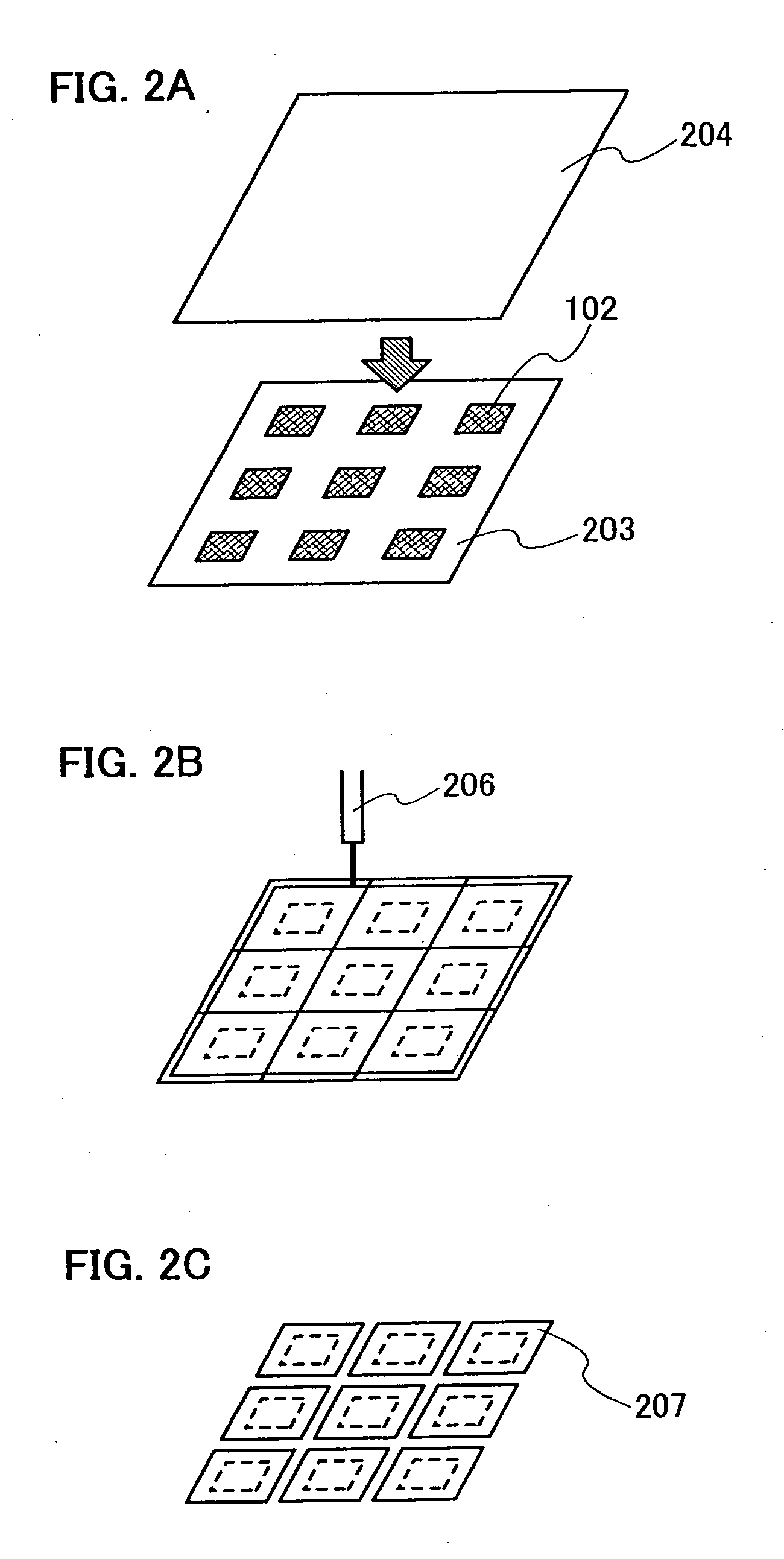
[0086] In Embodiment 1, an embodiment of a process up to arranging regularly a plurality of thin film integrated circuits 102 over the first film 203 is described.

[0087] First, a substrate 400 is prepared and a release layer 401 is formed over the substrate 400 as shown in FIG. 4A. Here, a release layer means a layer for facilitating releasing the plurality of thin film integrated circuits 102 from the substrate 400. Specifically, a glass substrate of, for example, barium borosilicate glass, aluminoborosilicate glass, a quartz substrate, a ceramic substrate, or the like can be used as the substrate 400. Further, a metal substrate such as stainless steel or a semiconductor substrate provided with an insulating film on its surface may also be used. Although a substrate made of a flexible plastic generally tends to have lower heat-resistance than the above-described substrate, it can be used as the substrate 400 as long as it can withstand process temperature in the manufacturing proc...

embodiment 2

[0108] In Embodiment 2, a method of using a film having an adhesive agent on one side thereof when the thin film integrated circuits 408 on the substrate 400 are transferred onto the first film 203 as shown in Embodiment 1, is described with reference to FIGS. 14A to 14C.

[0109] A state in FIG. 4E or 5 is obtained according to the method shown in Embodiment 1. Then, the thin film integrated circuits 408 are bonded to a film 407 as shown in FIG. 14A by positioning the film 407 having an adhesive layer 406 on one side of a base 405 over the thin film integrated circuit 408 so that the adhesive layer 406 can be in contact with the thin film integrated circuit 408, and pressing them from above the thin film integrated circuit 408. FIG. 14A shows an example of bonding the thin film integrated circuits 408 to the film 407 in the state of FIG. 5.

[0110] The film 407 may have, specifically, a structure in which the adhesive layer 406 is provided on the base 405 formed of polyester, or the l...

embodiment 3

[0116] Embodiment 3 describes a process up to a state in which a plurality of thin film integrated circuits are arranged over the first film 203 as shown in FIG. 2A, which is different from that in Embodiment 1.

[0117] A layer 901 including a plurality of thin film integrated circuits (hereinafter, a TFT layer 901) is formed over one surface of a substrate 900 having an insulating surface (FIG. 9A). The substrate 900 corresponds to a glass substrate such as barium borosilicate glass or alumino borosilicate glass, a quartz substrate, a ceramic substrate, a plastic substrate, an acrylic substrate, or the like. A metal substrate such as stainless steel or a semiconductor substrate having an insulating layer on its surface may also be used. The substrate 900 can be easily manufactured to have a length of 1 m or more on a side, and can have a desired shape such as a square or circular shape. Therefore, when the substrate 900 has a size of 1 m or more on a side, for example, the productiv...


PUM


Abstract

The present invention provides a new type wireless chip that can be used without being fixed on a product. Specifically, a wireless chip can have a new function by a sealing step. One feature of a wireless chip according to the present invention is to have a structure in which an integrated circuit is sealed by films. In particular, the films sealing the integrated circuit have a hollow structure; therefore the wireless chip can have a new function.

Description

BACKGROUND OF THE INVENTION [0001] 1. Field of the Invention [0002] The present invention relates to a wireless chip and a manufacturing method of the wireless chip. [0003] 2. Description of the Related Art [0004] In recent years, a wireless chip for transmitting and receiving data has been actively developed and such a wireless chip is called, e.g., an IC tag, an ID tag, an RF (Radio Frequency) tag, a wireless tag, an electronic tag, a wireless processor, a wireless memory. For a transmission system of a wireless chip, there are three systems of an electromagnetic coupling system, an electromagnetic induction system and a radio wave system. The electromagnetic coupling system employs a mutual induction of electric coils by alternating magnetic field, and employs a frequency of 13.56 MHz. The electromagnetic induction system employs two frequencies with classifying broadly. One is 135 kHz or less and the other is 13.56 MHz. Communication having a range of maximum 1 m with a wireless...

Claims


Application Information

Patent Timeline
IPC IPC(8): H01L23/02H01L23/24
CPCH01L21/6835H01L23/20H01L2924/00011H01L2224/293H01L2224/2929H01L2924/01079H01L2924/01019H01L23/22H01L23/58H01L24/83H01L2221/6834H01L2221/68363H01L2221/68368H01L2224/83851H01L2924/09701H01L2924/19041H01L2924/30105H01L2224/29075H01L2924/00014H01L2924/12042H01L2924/14H01L2924/00
Inventor TSURUME, TAKUYADAIRIKI, KOJIKUSUMOTO, NAOTO
Owner SEMICON ENERGY LAB CO LTD
Why Eureka
Try Eureka