Organic light emitting display

a light emitting display and organic technology, applied in static indicating devices, instruments, electroluminescent light sources, etc., can solve the problems of non-uniform brightness deviations between threshold voltages of driving transistors, and inability to meet the requirements of light emitting displays, so as to enhance the picture quality of organic light emitting displays, reduce leakage current, and uniform light emitting displays

Active Publication Date: 2006-03-16
SAMSUNG DISPLAY CO LTD
View PDF11 Cites 87 Cited by
  • Summary
  • Abstract
  • Description
  • Claims
  • Application Information

AI Technical Summary

Benefits of technology

[0016] Accordingly, an embodiment of the present invention provides a pixel and an organic light emitting display, in which a current flows through a driving transistor regardless of a threshold voltage of the driving transistor, so that a difference between threshold voltages of driving transistors is compensated, thereby a brightness of the organic light emitting display is more uniform. In another embodiment, a pixel and an organic light emitting display further enhance a picture quality of the organic light emitting display by reducing a leakage current.

Problems solved by technology

However, when a conventional organic light emitting display is fabricated, a deviation may arise between threshold voltages of driving transistors (e.g., the driving transistor M2).
The deviation between the threshold voltages of the driving transistors causes the intensity of currents flowing into organic light emitting diodes OLEDs to be not uniform, so that the conventional organic light emitting display displays an image with non-uniform brightness.

Method used


Image

  • Organic light emitting display
  • Organic light emitting display
  • Organic light emitting display

Examples


Embodiment Construction

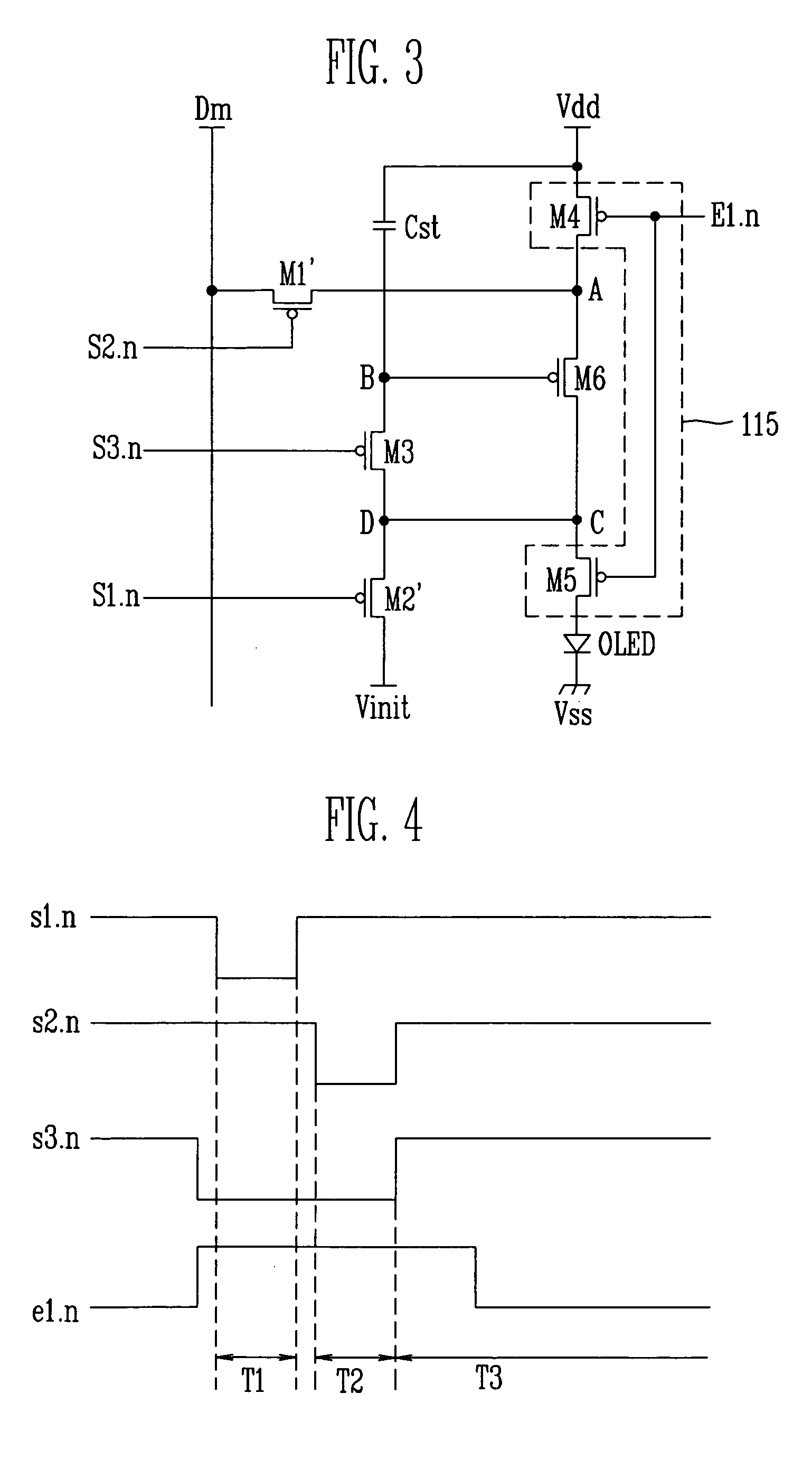
[0029] Hereinafter, certain exemplary embodiments according to the present invention will be described with reference to the accompanying drawings. The exemplary embodiments of the present invention are provided to be readily understood by those skilled in the art.

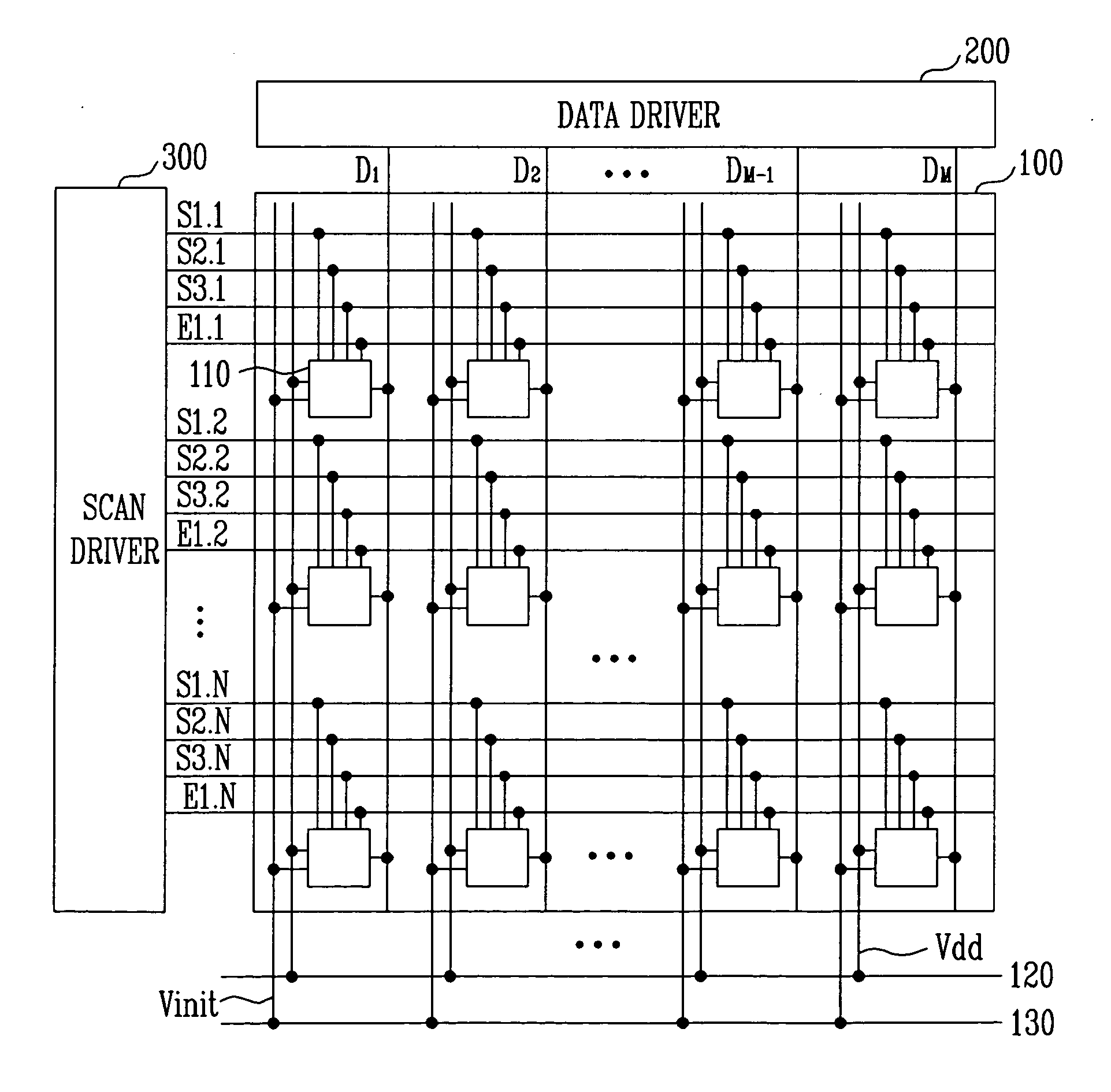
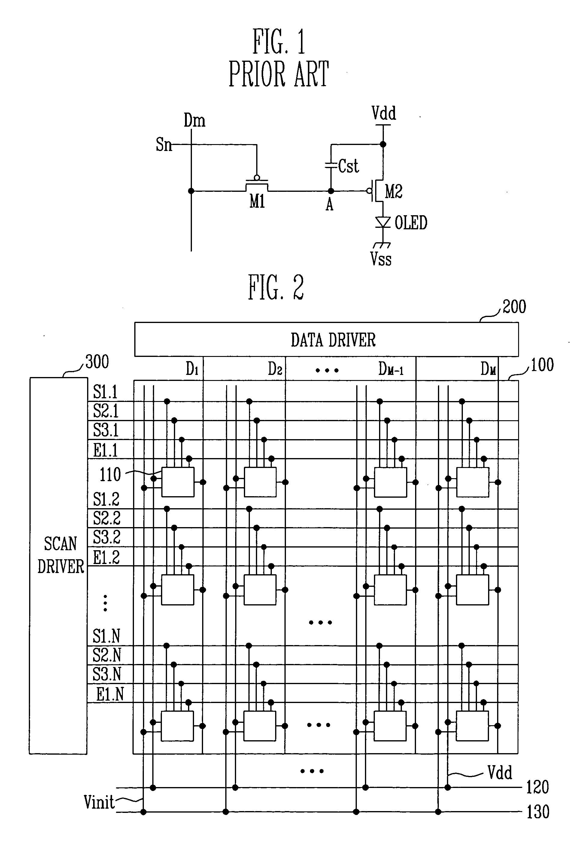
[0030]FIG. 2 illustrates a configuration of an organic light emitting display according to an embodiment of the present invention. Referring to FIG. 2, the organic light emitting display according to the embodiment of the present invention includes a pixel part 100, a data driver 200, and a scan driver 300.

[0031] The pixel part 100 includes N×M pixels 110 having organic light emitting diodes OLED; N first scan lines S1.1, S1.2, . . . , S1.N−1, S1.N arranged in a row direction; N second scan lines S2.1, S2.2, . . . , S2.N−1, S2.N arranged in the row direction; N third scan lines S3.1, S3.2, . . . , S3.N−1, S3.N arranged in the row direction; N emission control lines E1.1, E1.2, . . . , E1.N−1, E1.N arranged in the row dir...


PUM


Abstract

An organic light emitting display includes a plurality of pixels, at least one of the pixels having: an organic light emitting diode; a driving transistor adapted to supply a driving current to the organic light emitting diode; a first switching transistor adapted to selectively supply a data signal to the driving transistor; a second switching transistor adapted to selectively supply an initialization signal; a third switching transistor adapted to selectively allow the driving transistor to be connected as a diode and to selectively supply the initialization sought; a storage capacitor adapted to store a first voltage corresponding to the initialization signal received from the third switching transistor and then to store a second voltage corresponding to the data signal applied at a gate electrode of the driving transistor; and an interrupter adapted to selectively supply a pixel power to the driving transistor and to selectively allow the driving current to flow into the organic light emitting diode. In this display, the amount of current leaking out through a switching transistor is decreased, and thus a voltage variance applied to a gate electrode of a driving transistor is decreased, thereby enhancing a contrast of an image.

Description

CROSS-REFERENCE TO RELATED APPLICATION [0001] This application claims priority to and the benefit of Korean Patent Application No. 10-2004-0068405, filed on Aug. 30, 2004, in the Korean Intellectual Property Office, the entire content of which is incorporated herein by reference. BACKGROUND [0002] 1. Field of the Invention [0003] The present invention relates to an organic light emitting display, and more particularly, to an organic light emitting display which compensates a threshold voltage of a driving transistor to improve a uniformity in brightness. [0004] 2. Discussion of Related Art [0005] Recently, various flat panel displays, which are thinner than a comparable cathode ray tube display, have been developed. As a flat panel display, an organic light emitting display has excellent emission efficiency, brightness and viewing angle, as well as a fast response time. [0006] An organic light emitting diode (OLED) of an organic light emitting display has a structure that includes a...

Claims


Application Information

Patent Timeline
Patent Type & Authority Applications(United States)
IPC IPC(8): G09G3/10G09G3/30H05B44/00
CPCG09G3/3233G09G2300/0819G09G2320/043G09G2300/0861G09G2320/0233G09G2300/0842G09G3/30
Inventor JEONG, JIN TAE
Owner SAMSUNG DISPLAY CO LTD
Why Eureka
Try Eureka