Light emitting display device, electronic equipment into which the same device is loaded, and drive method of the light emitting display device

Inactive Publication Date: 2006-03-16
TOHOKU PIONEER CORP
View PDF4 Cites 0 Cited by
  • Summary
  • Abstract
  • Description
  • Claims
  • Application Information

AI Technical Summary

Benefits of technology

[0019] The present invention has been developed based on the above-described technical viewpoint, and it is an object of the present invention to provide a light emitting display device equipped with pixel circuits which can suppress variations of light emission intensities generated among pixels by correcting threshold characteristics of light emission drive transistors constituting light emitting pixels within respective pixels, and particularly to provide a light emitting display device equipped with the pixel circuits which can be appropriately adopted in a structure of the SES method already described and the drive method thereof.

Problems solved by technology

Such variations in light emission intensities among pixels allow, particularly when an animation image and the like is reproduced, a vague stripe pattern or a phenomenon resembling flicker to be generated, thereby causing a problem that display quality is considerably degraded.
However, regarding this, there exist a number of technical problems including a problem of selection of a semiconductor material or other materials, a problem of a manufacturing process, a problem of a manufacturing environment, and the like, and it is difficult to pursue a fundamental solution.

Method used


Image

  • Light emitting display device, electronic equipment into which the same device is loaded, and drive method of the light emitting display device
  • Light emitting display device, electronic equipment into which the same device is loaded, and drive method of the light emitting display device
  • Light emitting display device, electronic equipment into which the same device is loaded, and drive method of the light emitting display device

Examples


Embodiment Construction

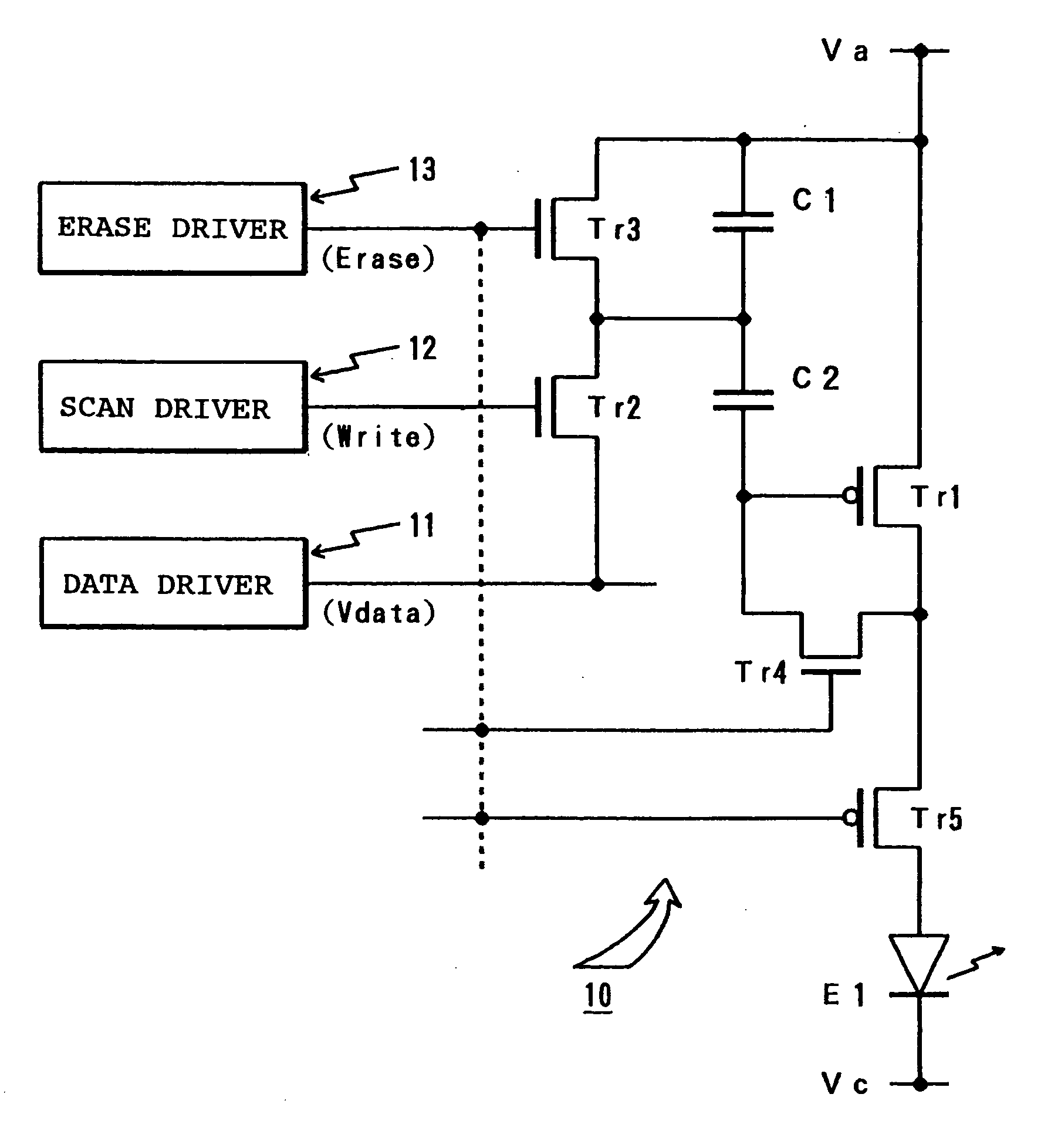
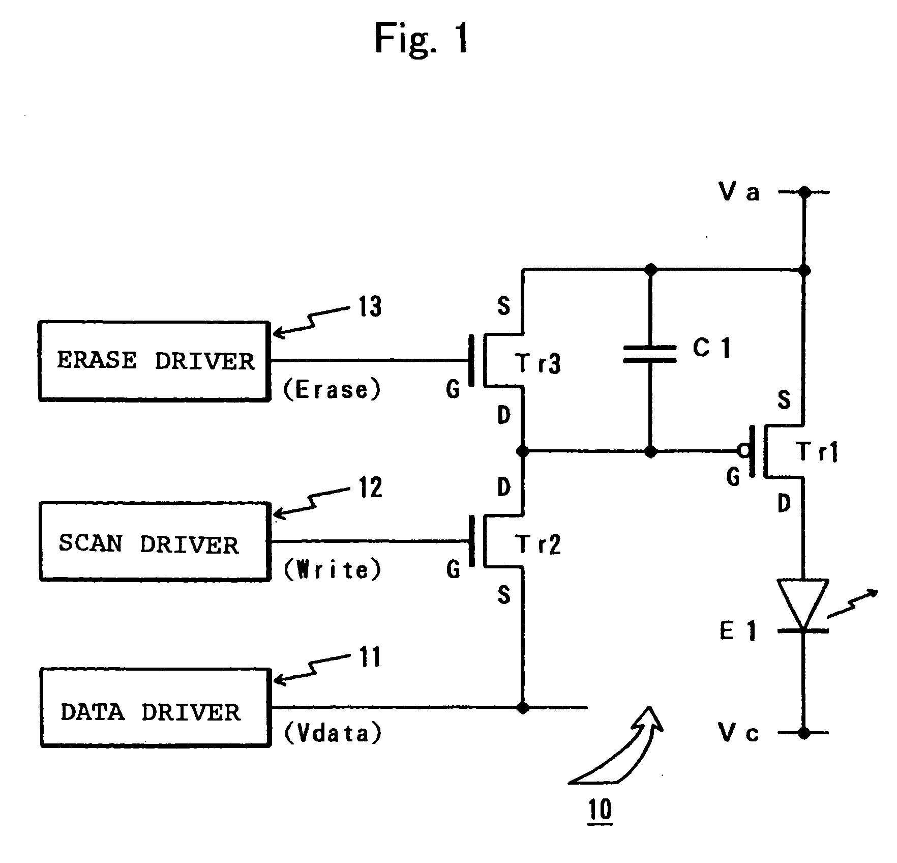
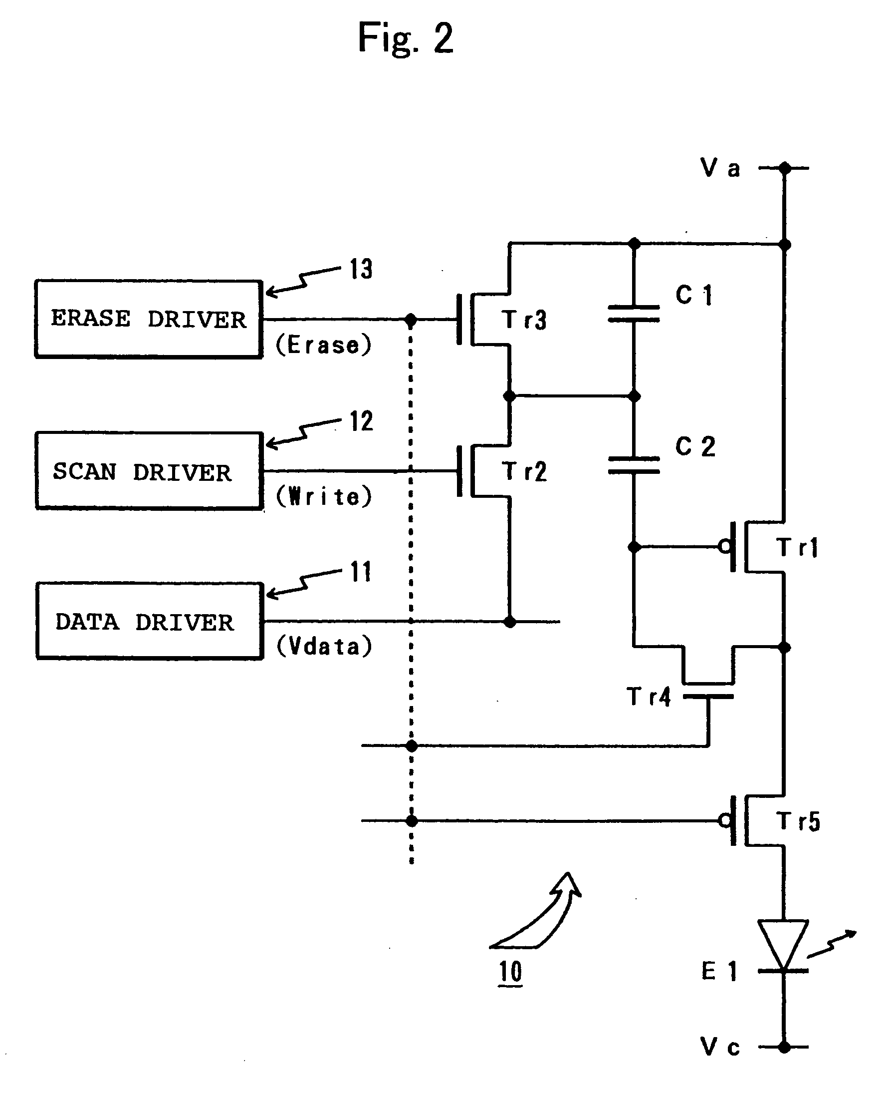
[0026] A light emitting display device and the drive method thereof according to the present invention will be described below based on an embodiment shown in the drawings. Any of FIGS. 2-4 show an embodiment of a light emitting display device according to the present invention, and FIG. 2 explains a structure of one pixel 10. FIG. 3 explains a state in which a correction voltage is written in the same pixel structure, and further FIG. 4 shows a state in which data writing is performed in the same pixel structure and shows a state which follows this and in which an EL element as a light emitting element is driven to emit light.

[0027] First, in the structure shown in FIG. 2, the respective data driver 11, scan driver 12, erase driver 13, light emission drive transistor Tr1, data write transistor Tr2, erase transistor Tr3, light emission maintaining capacitor C1, organic EL element E1 as a light emitting element, anode side drive power source Va, and cathode side drive power source V...


PUM


Abstract

A correction voltage retaining capacitor C2, a correction voltage write transistor Tr4, and a switching transistor Tr5 are added to a pixel structure of an SES drive method provided with an organic EL element E1 as a light emitting element, a light emission drive transistor Tr1, a data write transistor Tr2, and an erase transistor Tr3 which can erase electrical charges in a light emission maintaining capacitor C1. With the ON operation of the erase transistor Tr3, the correction voltage write transistor Tr4 is turned on, and the switching transistor Tr5 is turned off. In this state, the threshold voltage (Vth) of the light emission drive transistor Tr1 is written in the correction voltage retaining capacitor C2. When pixels are lit, by a gate-to-source voltage obtained by adding the threshold voltage written in the correction voltage retaining capacitor C2 to a data voltage written in the light emission maintaining capacitor C1, drain current of the light emission drive transistor Tr1 flows. Thus, among respective pixels, a lighting operation is performed in a state in which variations of light emission intensities caused by variations of threshold voltages of the light emission drive transistor Tr1 are restrained.

Description

BACKGROUND OF THE INVENTION [0001] 1. Field of the Invention [0002] The present invention relates to a light emitting display device in which light emitting elements constituting pixels are actively driven for example by TFTs (Thin Film Transistors) and in particular to a light emitting display device which can effectively restrain intensity non-uniformity among respective pixels which occurs due to variations in characteristics of light emission drive transistors that give drive current to the respective light emitting elements. [0003] 2. Description of the Related Art [0004] Demand for a display panel which has a high definition image display function and which can realize a thin shape and low power consumption has increased due to popularity of cellular telephones, personal digital assistants (PDAS), and the like, and conventionally a liquid crystal display panel has been adopted in many products as the one which meets the needs thereof. Meanwhile, these days a self light emittin...

Claims


Application Information

Patent Timeline
IPC IPC(8): G09G3/36H05B44/00
CPCG09G3/2022G09G3/3233G09G2300/043G09G2320/0233G09G2300/0852G09G2300/0861G09G2300/0819
Inventor SEKI, SHUICHI
Owner TOHOKU PIONEER CORP
Why Eureka
Try Eureka