Semiconductor physical quantity sensor and method for manufacturing the same

a technology of magnetic field and sensor, which is applied in the direction of turn-sensitive devices, capacitors with electrode area variation, instruments, etc., can solve the problems of reducing the production field, affecting affecting the normal movement of the movable electrode, so as to improve the manufacturing yield of the sensor, increase the thickness of the insulation film, and increase the distance between the movable electrode and the substrate.

Inactive Publication Date: 2006-03-16
DENSO CORP
View PDF4 Cites 12 Cited by
  • Summary
  • Abstract
  • Description
  • Claims
  • Application Information

AI Technical Summary

Benefits of technology

[0022] In the above method, since the connection portion between the movable electrode and the substrate is cambered toward the direction apart from the substrate, the distance between the movable electrode and the substrate becomes larger, compared with the distance between the fixed electrode and the substrate. Thus, without increasing the thickness of the insulation film as a sacrifice layer, the distance between the movable electrode and the substrate becomes larger. Thus, even if a foreign particle is inserted between the movable electrode and the substrate, the motion of the movable electrode is not affected by the foreign particle. Thus, the movable electrode works normally. Accordingly, manufacturing yield of the sensor is improved.
[0026] In this case, since the movable electrode is shifted toward a direction apart from the substrate, the distance between the movable electrode and the substrate becomes larger, compared with the distance between the fixed electrode and the substrate. Thus, without increasing the thickness of the insulation film as a sacrifice layer, the distance between the movable electrode and the substrate becomes larger. Thus, even if a foreign particle is inserted between the movable electrode and the substrate, the motion of the movable electrode is not affected by the foreign particle. Thus, the movable electrode works normally. Accordingly, manufacturing yield of the sensor is improved.
[0029] In this case, the movable electrode is apart from the substrate by a predetermined distance, which is different from a distance between the fixed electrode and the substrate. Thus, without increasing the thickness of the insulation film as a sacrifice layer, the distance between the movable electrode and the substrate becomes larger. Thus, even if a foreign particle is inserted between the movable electrode and the substrate, the motion of the movable electrode is not affected by the foreign particle. Thus, the movable electrode works normally. Accordingly, manufacturing yield of the sensor is improved.

Problems solved by technology

However, in such a case that semiconductor physical quantity sensors having such a thin gap between these electrodes and the support substrates are manufactured, there are some possibilities that foreign matters such as particles are mixed in this gap in the manufacturing stage thereof.
Thus, the normal movement of the movable electrode is impeded.
As previously explained, the mixture of the foreign matters may conduct problems in sensor characteristics, and also, may lower the field of the production.
However, generally speaking, since the SOI wafers having the thick thicknesses of the embedded oxide films as the sacrifice layers become high cost, the use of these SOI wafers is not desirable.

Method used


Image

  • Semiconductor physical quantity sensor and method for manufacturing the same
  • Semiconductor physical quantity sensor and method for manufacturing the same
  • Semiconductor physical quantity sensor and method for manufacturing the same

Examples


first embodiment

[0046] A capacitance type semiconductor physical quantity sensor according to a first embodiment of the present invention is applied to a capacitance type angular rate sensor.

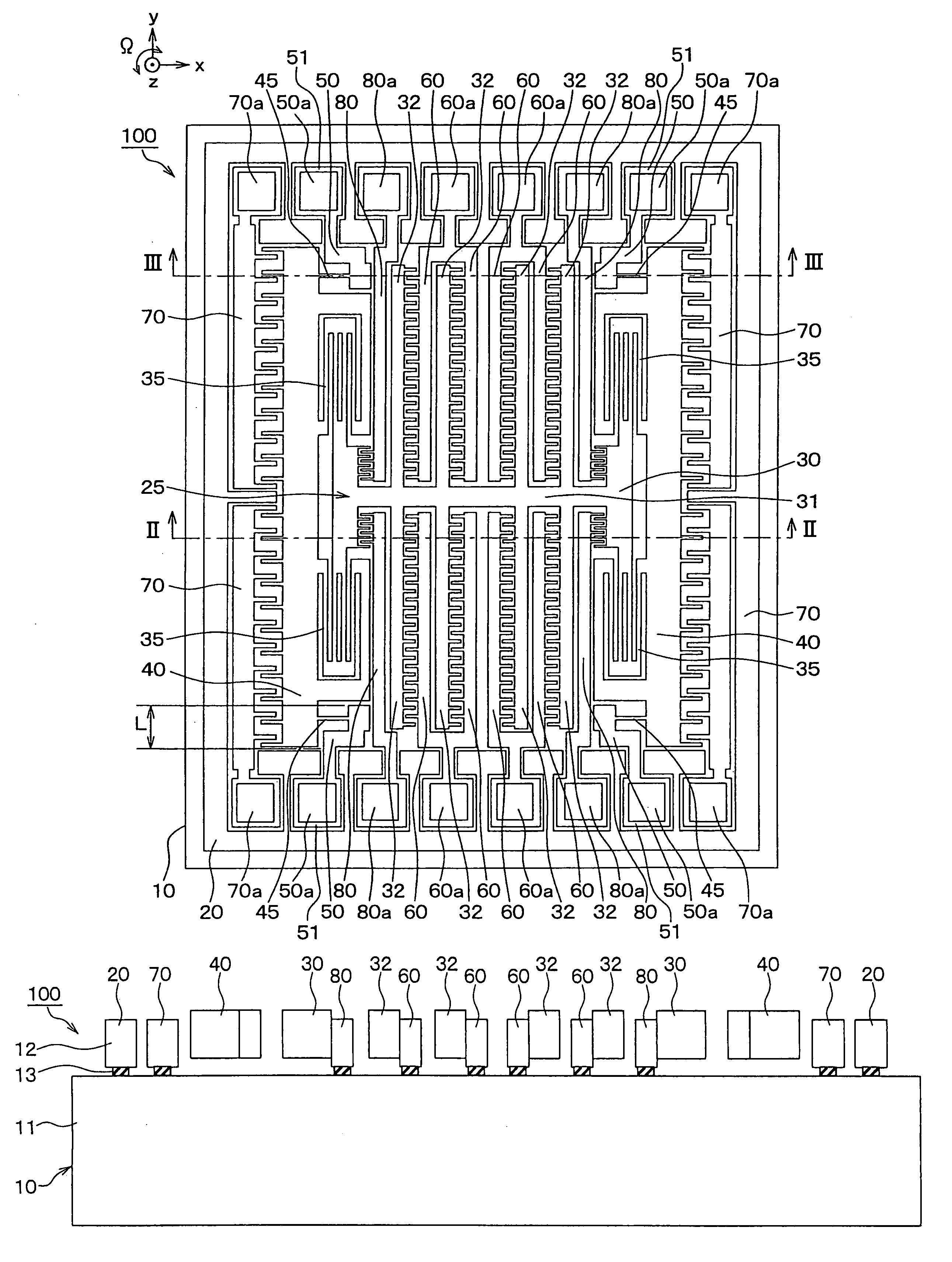
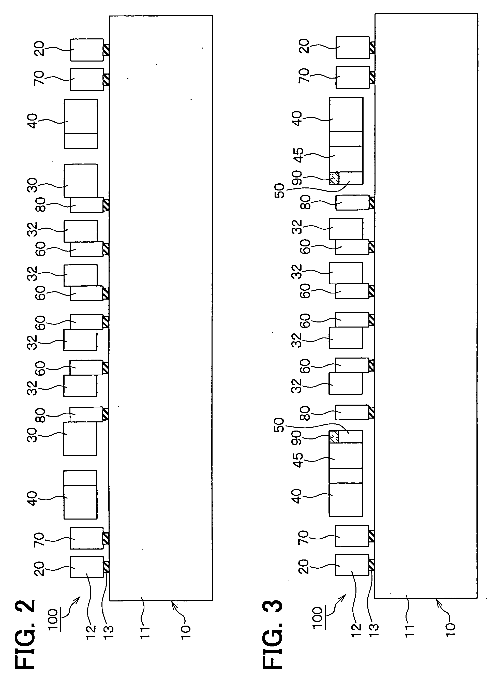
[0047]FIG. 1 is a plan view for schematically showing a capacitance type angular rate sensor 100 according to the first embodiment. Also, FIG. 2 is a sectional view for schematically indicating the capacitance type angular rate sensor 100, taken along a line II-II of FIG. 1. FIG. 3 is a sectional view for schematically showing the angular rate sensor 100, taken along a line III-III of FIG. 1.

[0048] [Structure]

[0049] This angular rate sensor 100 is made of a semiconductor substrate 10 such as a silicon substrate. Since trenches are formed in this semiconductor substrate 10 by employing the well-known semiconductor manufacturing technique such as an etching process, as indicated in FIG. 1, a frame unit 20 is segmented to be formed in an outer peripheral unit of this semiconductor substrate 10 and also, a movabl...

second embodiment

[0158]FIG. 9 is a diagram for schematically showing a sectional structure of a capacitance type angular rate sensor 200 according to a second embodiment of the present invention.

[0159] A plane structure of the angular rate sensor 200 is made similar to the plane structure shown in FIG. 1. FIG. 9 represents the angular rate sensor 200 by way of the sectional view shown in FIG. 2, namely, such a sectional view corresponding to the sectional view taken along the line II-II in FIG. 1.

[0160] In the angular rate sensor 100 shown in FIG. 1 to FIG. 3, the substantially entire portions of the fixed electrodes 60, 70, 80 are supported via the embedded oxide film 13 by the silicon substrate 11 to be fixed thereon (refer to FIG. 2 and FIG. 3).

[0161] To the contrary, in the angular rate sensor 200, the fixed electrodes 60 to 80 are supported via the embedded oxide film 13 at respective portions which are located in the peripheral unit of the silicon substrate 11, at portions where the pads 60...

third embodiment

[0169]FIG. 10 is a diagram for schematically showing a sectional structure of a capacitance type angular rate sensor 300 according to a third embodiment of the present invention.

[0170] A plane structure of the angular rate sensor 300 is made similar to the plane structure shown in FIG. 1. FIG. 10 represents the angular rate sensor 300 mode by way of the sectional view shown in FIG. 2, namely, such a sectional view corresponding to the sectional view taken along the line II-II in FIG. 1.

[0171] Similar to the angular rate sensor 200 shown in FIG. 9, in the angular rate sensor 300, the fixed electrodes 60 to 80 are supported via the embedded oxide film 13 at respective portions which are located in the peripheral unit of the silicon substrate 11, at portions where the pads 60a to 80a are formed under cantilever conditions.

[0172] This angular rate sensor 300 is featured by that the fixed electrodes 60 to 80 are coupled under such a condition that these fixed electrodes 60 to 80 are s...


PUM


Abstract

A method for manufacturing a semiconductor physical quantity sensor including a support substrate, a movable electrode, a fixed electrode is provided. The method includes the steps of: preparing a multi-layered substrate; forming a compression stress layer on a part of a surface of the semiconductor layer; forming a trench in the semiconductor layer; and releasing the movable electrode from the substrate by removing the insulation film. In the step of releasing, the part of the semiconductor layer, on which the compression stress layer is disposed, is cambered by the compression stress toward a direction apart from the substrate.

Description

CROSS REFERENCE TO RELATED APPLICATION [0001] This application is based on Japanese Patent Application No. 2004-269540 filed on Sep. 16, 2004, the disclosure of which is incorporated herein by reference. FIELD OF THE INVENTION [0002] The present invention relates to a semiconductor physical quantity sensor and a method for manufacturing the same. BACKGROUND OF THE INVENTION [0003] A capacitance type semiconductor physical quantity sensor includes a movable electrode and a fixed electrode located opposite to the movable electrode, which are formed on a support substrate. A physical quantity is detected based upon a capacitance change between the movable electrode and the fixed electrode. [0004] Generally speaking, this sort of semiconductor physical quantity sensor is equipped with a movable electrode and a fixed electrode, and detects a physical quantity based upon a capacitance change between the movable electrode and the fixed electrode when a physical quantity is applied to this ...

Claims


Application Information

Patent Timeline
Patent Type & Authority Applications(United States)
IPC IPC(8): H01L21/00G01C19/56G01C19/5762G01C19/5769G01P15/08G01P15/125H01L29/84
CPCB81B2201/0235B81B2201/0242H01L31/18B81C1/00952B81C2201/0167B81B2203/0136
Inventor YOKOYAMA, KENICHI
Owner DENSO CORP
Why Eureka
Try Eureka