Growth of III-nitride light emitting devices on textured substrates

a technology of textured substrates and light emitting devices, which is applied in the direction of semiconductor/solid-state device manufacturing, semiconductor devices, electrical devices, etc., can solve the problems of significant attenuation of light and poor extraction efficiency, and achieve the effects of reducing the amount of total internal reflection, improving material quality, and high quality

Active Publication Date: 2006-03-23
LUMILEDS
View PDF13 Cites 43 Cited by
  • Summary
  • Abstract
  • Description
  • Claims
  • Application Information

AI Technical Summary

Benefits of technology

[0006] In accordance with embodiments of the invention, a III-nitride light emitting device is grown on a textured substrate, in order to reduce the amount of total internal reflection at the interface between the substrate and the III-nitri

Problems solved by technology

The use of a sapphire substrate may lead to poor extraction efficiency due to the large difference in index of refraction at the interface between the semiconductor layers and the substrate.
Th

Method used


Image

  • Growth of III-nitride light emitting devices on textured substrates
  • Growth of III-nitride light emitting devices on textured substrates
  • Growth of III-nitride light emitting devices on textured substrates

Examples


Embodiment Construction

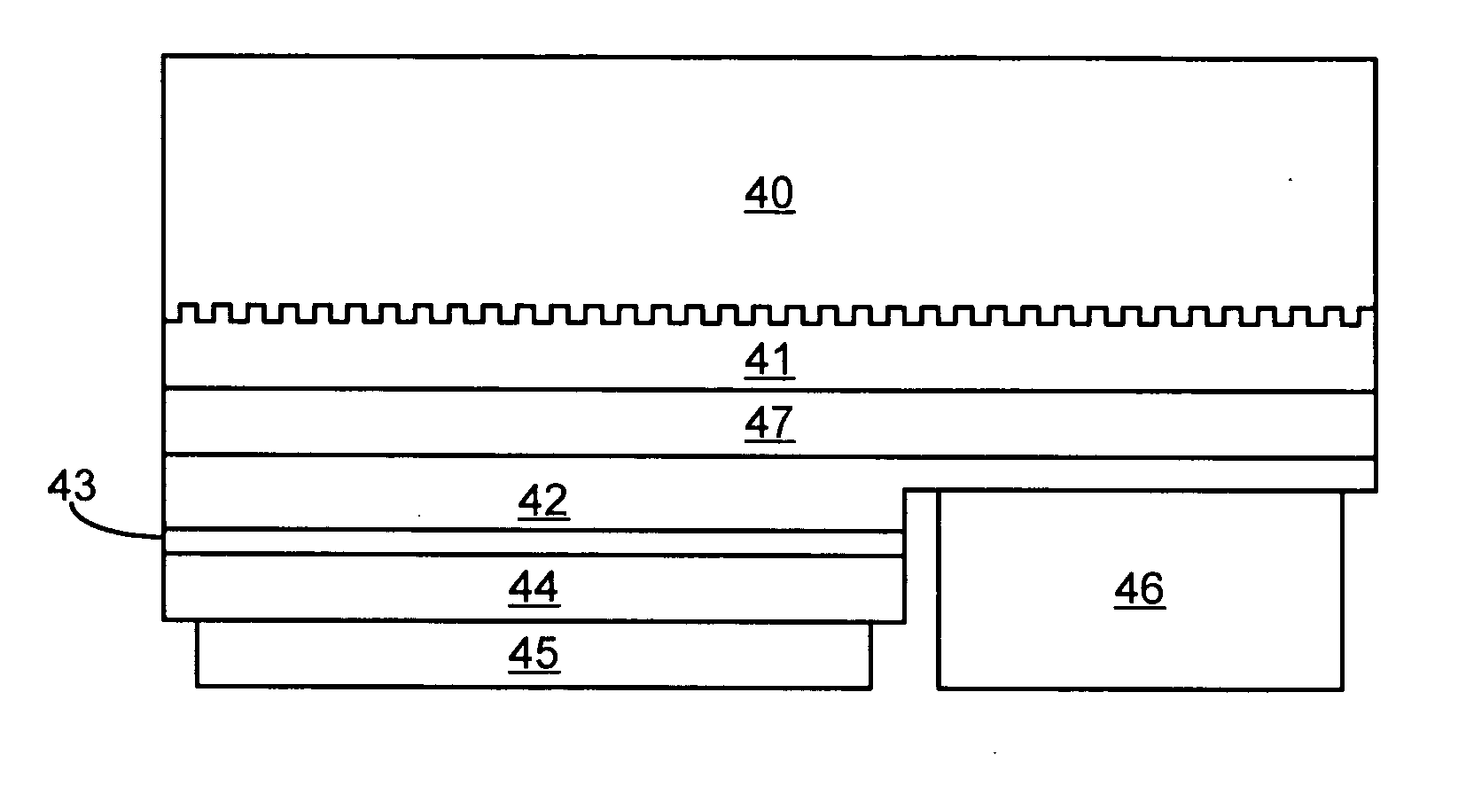
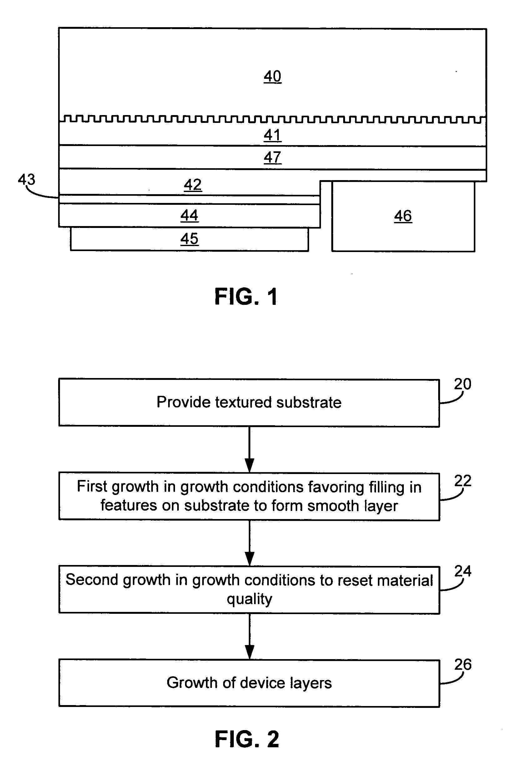
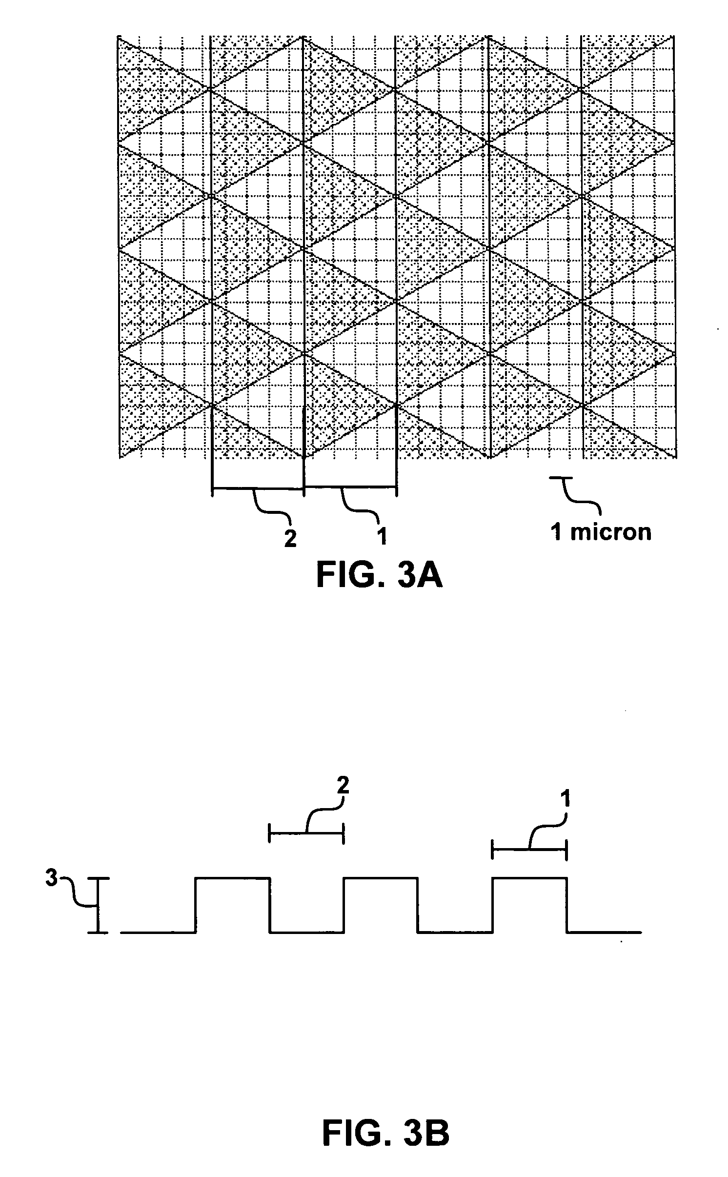
[0013] Total internal reflection at the interface between a sapphire or other suitable substrate and the III-nitride device layers may be reduced by texturing or patterning the substrate. As used herein, “textured” refers to a substrate surface that is not smooth, either due to random roughening of the surface or due to forming a pattern of repeating features on the surface. For economy of language, many of the examples below refer to patterned substrate surfaces. It is to be understood that the same principles may be applied to devices with randomly roughened substrate surfaces. A patterned substrate generally has a thickness that varies with the pattern. As used herein, a “feature” on a patterned substrate refers to the parts of the pattern where the substrate is thicker than the minimum substrate thickness. For example, if a pattern on a substrate includes triangular regions where the substrate is thick interposed by triangular regions where the substrate is thinner, as illustrat...


PUM


Abstract

A III-nitride light emitting device is grown on a textured substrate, in order to reduce the amount of total internal reflection at the interface between the substrate and the III-nitride layers. In some embodiments, the device includes a first growth region substantially free of voids, and a second growth region that improves the material quality such that high quality layers can be grown over the first and second regions.

Description

BACKGROUND [0001] 1. Field of Invention [0002] The present invention relates to the growth of III-nitride light emitting devices. [0003] 2. Description of Related Art [0004] Semiconductor light-emitting diodes (LEDs) are among the most efficient light sources currently available. Materials systems currently of interest in the manufacture of high-brightness LEDs capable of operation across the visible spectrum include Group III-V compound semiconductors, particularly binary, ternary, and quaternary alloys of gallium, aluminum, indium, and nitrogen, also referred to as III-nitride materials. Such devices typically have a light emitting or active region sandwiched between a p-doped region and an n-doped region. The active region may be a single light emitting layer or multiple quantum well layers separated by barrier layers. Often III-nitride devices are epitaxially grown on sapphire, silicon carbide, or III-nitride substrates by metal organic chemical vapor deposition (MOCVD), molecul...

Claims


Application Information

Patent Timeline
IPC IPC(8): H01L31/109H01L33/00H01L33/02H01L33/08
CPCH01L21/02378H01L21/0242H01L21/0243H01L21/02458H01L33/22H01L21/0262H01L33/007H01L33/08H01L33/20H01L21/0254
Inventor KIM, ANDREW Y.MARANOWSKI, STEVEN A.
Owner LUMILEDS
Why Eureka
Try Eureka