Power factor correction circuit
- Summary
- Abstract
- Description
- Claims
- Application Information
AI Technical Summary
Benefits of technology
Problems solved by technology
Method used
Image

Examples
Embodiment Construction
[0034] The embodiments of the present invention and their advantages are best understood by referring to FIGS. 4 through 10 of the drawings. Like numerals are used for like and corresponding parts of the various drawings.
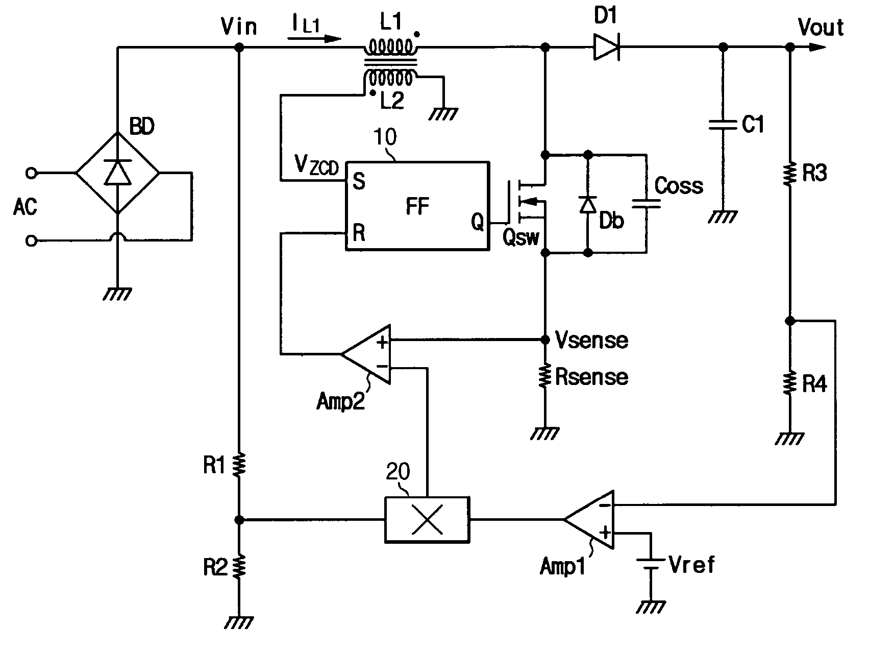
[0035]FIG. 4 is a schematic diagram of an exemplary implementation of power factor correction circuit 10, according to an embodiment of the present invention.
[0036] As depicted, the power factor correction circuit 10 may include a bridge diode BD 12, a boost circuit 14 including a transformer 16 having a primary winding L118, a switch Qsw 20, a diode D122, a capacitor C124, and a switching controller 100. Hereinafter, the inductor 16, a switch Qsw 20, the diode D122, and the capacitor C124 will be referred to as “the boost circuit” for convenience of description.
[0037] The bridge diode BD 12 rectifies an externally input AC voltage and outputs a full-wave rectification voltage Vin. The switching controller 100 receives a sensed output voltage Vout′ and a voltage ...
PUM
 Abstract
Description
Claims
Application Information
PatSnap Eureka turns technology decisions into work you can execute. Powered by our Innovation Knowledge Graph, it runs expert workflows across engineering, life sciences, materials and intellectual property. Get your review-ready output in minutes.


