
MRAM sense amplifier having a precharge circuit and method for sensing

a pre-charge circuit and amplifier technology, applied in the field of magnetoresistive random access memories, can solve the problems of high voltage requirements, poor write endurance of flash memory 10sup>4/sup>-10sup>6/sup>cycles, slow program and erase times,

Active Publication Date: 2006-03-23
VLSI TECH LLC
View PDF12 Cites 19 Cited by
  • Summary
  • Abstract
  • Description
  • Claims
  • Application Information

AI Technical Summary

Problems solved by technology

Disadvantages of FLASH memory include high voltage requirements and slow program and erase times. Also, FLASH memory has a poor write endurance of 104-106 cycles before memory failure.
Hence, FLASH memory is limited in the dimensions to which it can be scaled.

Method used


Image

  • MRAM sense amplifier having a precharge circuit and method for sensing
  • MRAM sense amplifier having a precharge circuit and method for sensing
  • MRAM sense amplifier having a precharge circuit and method for sensing

Examples


Embodiment Construction

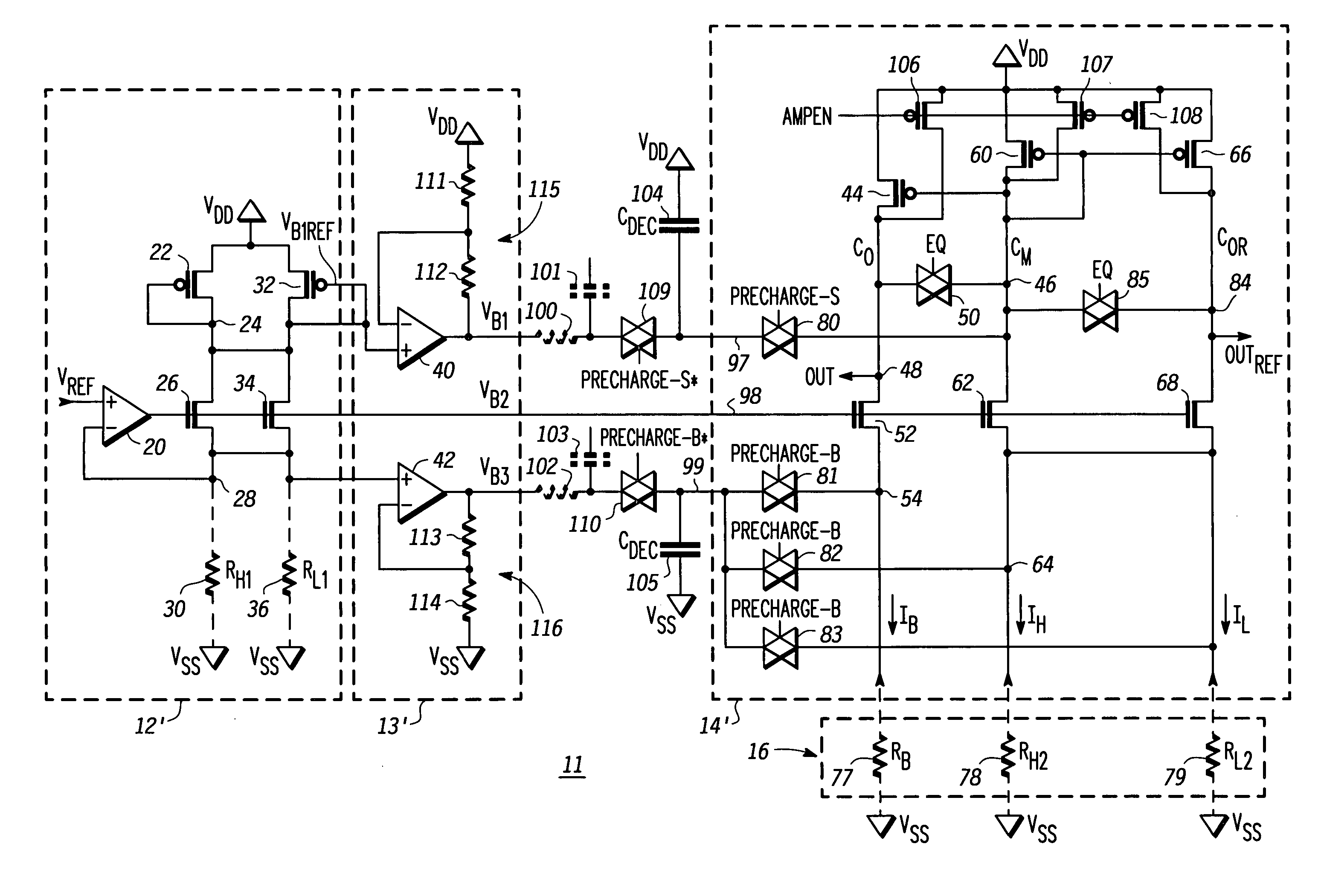
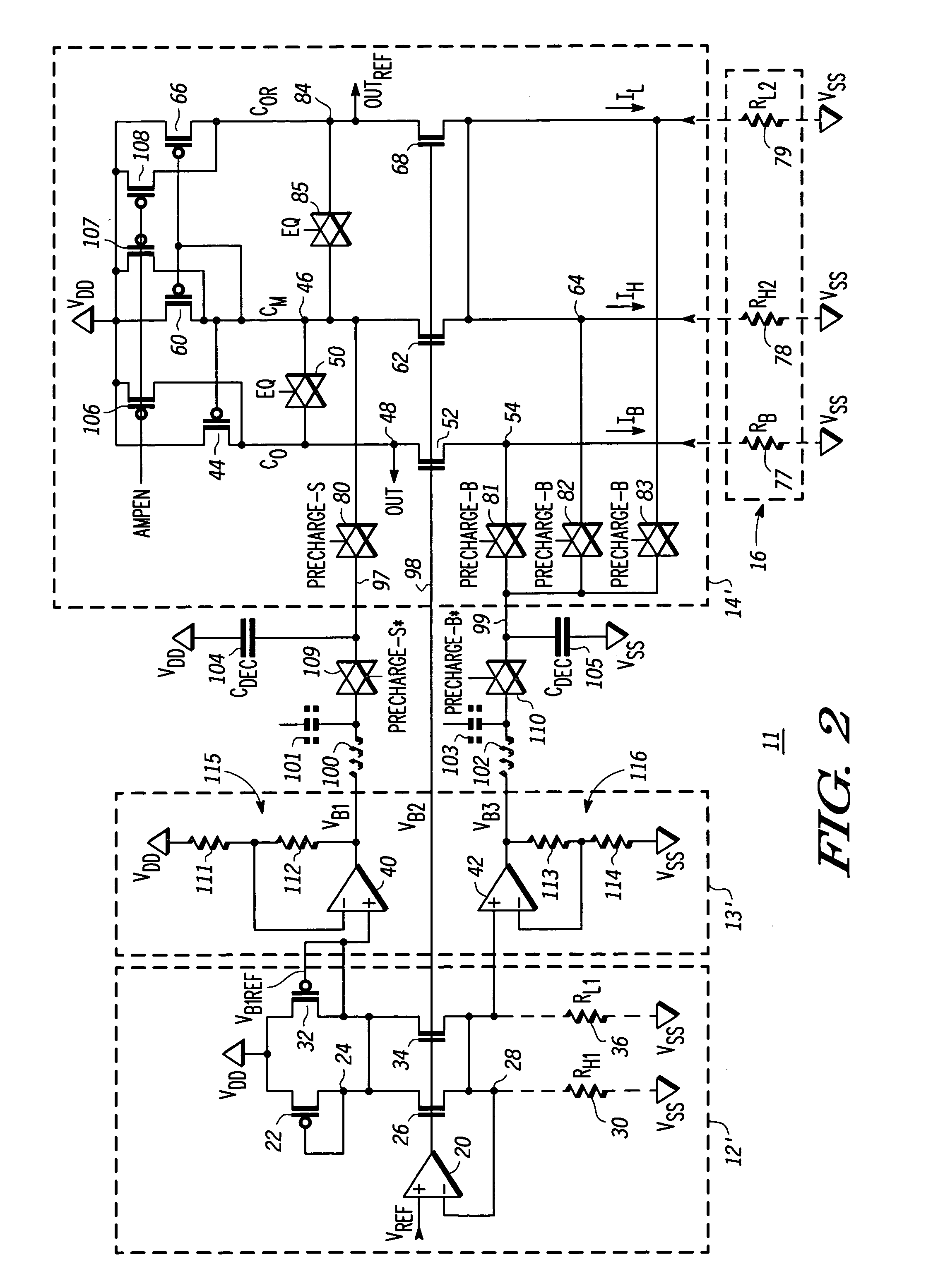
[0009] Generally, the present invention provides a sense amplifier and method for sensing a MRAM cell. The sense amplifier includes a precharge circuit that has an operational amplifier. The operational amplifier includes a voltage divider in its feedback path to control the amount of charge stored on a capacitor. During a precharge portion of a read operation, the charge stored on the capacitor is used to precharge the sense amplifier. A reference circuit defines a precharge voltage to which the sense amplifier is charged. By using charge sharing to precharge the sense amplifier, the sense amplifier can be precharged to a steady state common mode voltage more quickly, thus reducing the time for a read operation.

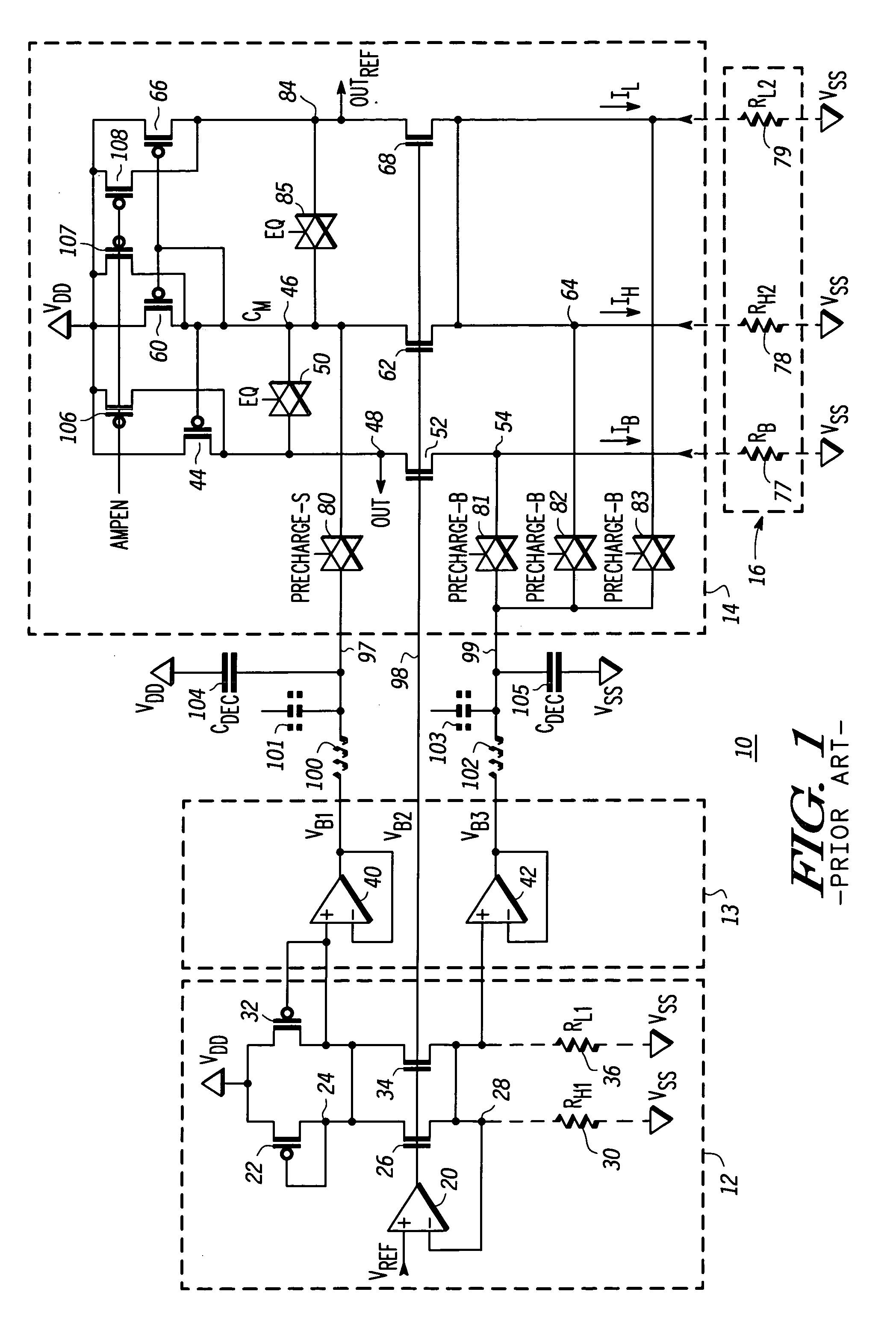
[0010]FIG. 1 illustrates, in schematic diagram form, a prior art MRAM sense amplifier 10. The MRAM sense amplifier 10 includes a reference circuit 12, a precharge circuit 13, and a sense circuit 14. The reference circuit 12 includes operational amplifier 20, P-channel trans...


PUM


Abstract

A sense amplifier (11) and method for sensing a MRAM cell (77) is provided. The sense amplifier (11) includes a precharge circuit (13′) having an operational amplifier (40, 42) that uses a voltage divider (115, 116) in a feedback path to control the amount of charge stored on a capacitor (104, 105). During a precharge portion of a read operation, the charge stored on the capacitor (104, 105) is used to precharge the sense amplifier (11). By using charge sharing to precharge the sense amplifier (11), the sense amplifier (11) can be precharged to a steady state common mode voltage more quickly, thus decreasing time required for a read operation.

Description

FIELD OF THE INVENTION [0001] This invention relates to Magnetoresistive Random Access Memories (MRAMs), and more particularly to a precharge and equalization circuit for an MRAM sense amplifier and method for sensing. BACKGROUND OF THE INVENTION [0002] Non-volatile memory devices, such as FLASH memories, are important components in electronic systems. FLASH is a major non-volatile memory device in use today. Disadvantages of FLASH memory include high voltage requirements and slow program and erase times. Also, FLASH memory has a poor write endurance of 104-106 cycles before memory failure. In addition, to maintain reasonable data retention, the scaling of the gate oxide is restricted by the tunneling barrier seen by the electrons. Hence, FLASH memory is limited in the dimensions to which it can be scaled. [0003] To overcome these shortcomings, magnetic memory devices are being evaluated. One such device is magnetoresistive RAM (hereinafter referred to as “MRAM”). To be commercially...

Claims


Application Information

Patent Timeline
IPC IPC(8): G11C7/02
CPCG11C11/16G11C7/062G11C5/14G11C7/06G11C11/15
Inventor GARNI, BRADLEY J.
Owner VLSI TECH LLC
Learn More