

Method of manufactruing circuit board
a manufacturing method and technology of circuit boards, applied in the direction of dielectric characteristics, conductive pattern formation, printed element electric connection formation, etc., can solve the problem that the resistance of a conductive paste in the hole accordingly increases, the electrical insulation between a conductive paste and an adjacent through-hole may be hardly obtained, and the material having a small porosity cannot be compressed at a high compressed rate, and achieves the effect of small rate and stable resistance of a conductive pas
- Summary
- Abstract
- Description
- Claims
- Application Information
AI Technical Summary
Benefits of technology
Problems solved by technology
Method used
Image

Examples
example 1
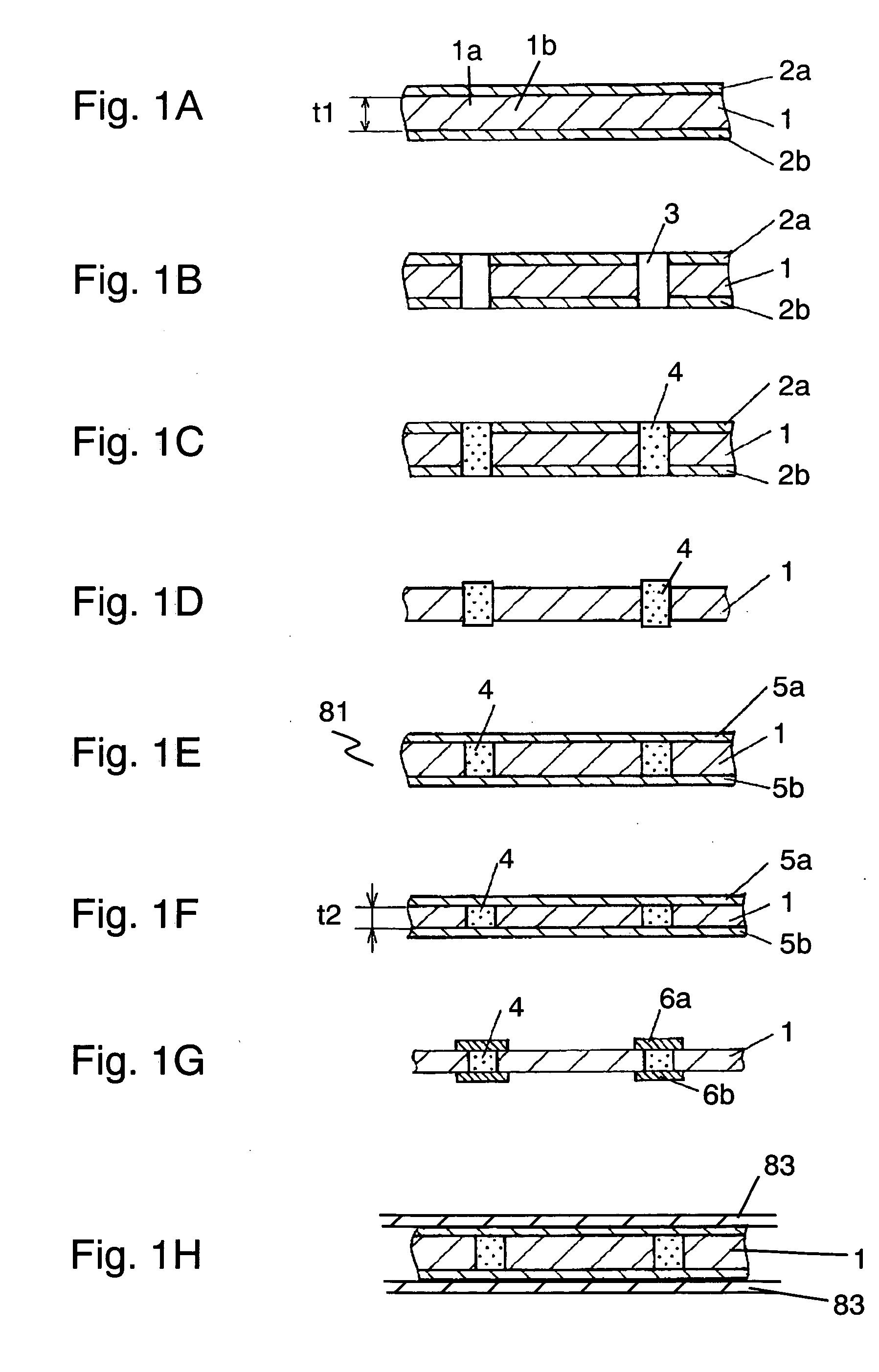
[0078] As shown in FIG. 1E, copper foils 5a and 5b having thicknesses of 18 μm were placed on pre-preg sheet 1 at a room temperature to provide laminated body 81. Ten sets of laminated bodies 81 were placed on a stainless mirror plate having a thickness of about 1 mm over a plate.
[0079] Laminated bodies 81 over the plate were put into a hot pressing machine, pressurized at pressure of 5 MPa for 10 minutes, and then taken out. Here, the hot pressing machine was a heating / pressurizing device having a temperature maintained at 70° C.
[0080] Next, as shown in FIG. 1F, laminated body 81 was heated according to temperature profile Tp1 shown in FIG. 3 by a vacuum hot pressing machine, pressurized at pressure of 5 MPa within resin flowing / hardening range R2 to be molded.
[0081] Laminated body 81 may be heated at 80° C. by a dryer as the heating device and put into the vacuum hot pressing machine.
[0082] By this method, a predetermined temperature-rising rate of laminated body 81 was obtain...
example 2
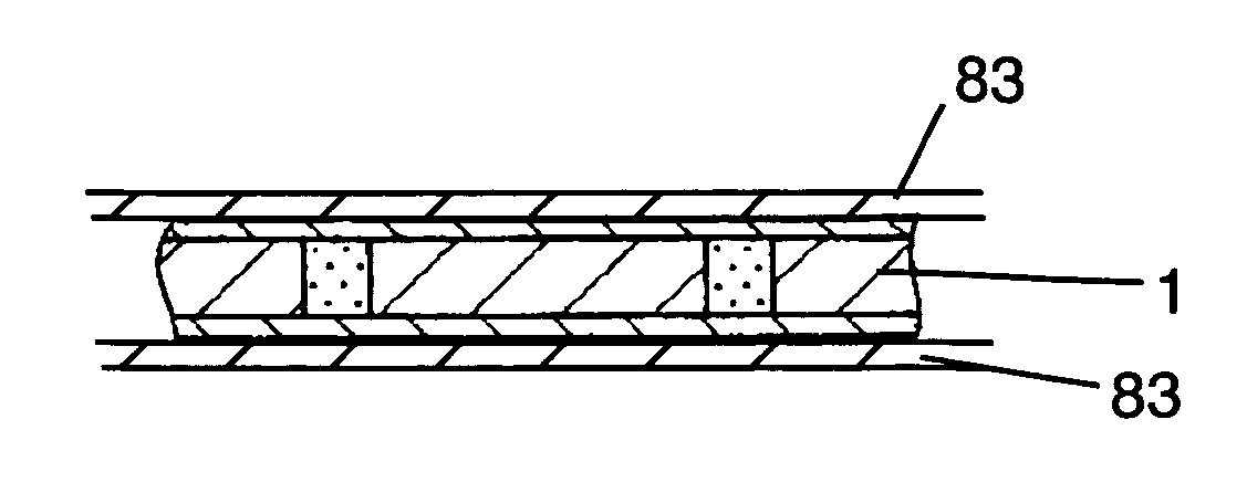
[0083] As shown in FIG. 1E, copper foils 105a and 105b having thicknesses of 18 μm were placed on pre-preg sheet 1 to provide laminated body 81. Then, as shown in FIG. 1H, each of 10 sets of laminated bodies 81 was sandwiched between stainless mirror plates 83 having thicknesses of about 1 mm, and was installed on a plate. Stainless mirror plates 83, a laminating device, were previously heated at 80° C. by a dryer.
[0084] Then, laminated body 81 was put into a vacuum hot pressing machine and heated according to temperature profile Tp1 shown in FIG. 3, and was pressurized at pressure of 5 MPa within resin flowing / hardening range R2 to be molded.
[0085] By this method, a predetermined temperature-rising rate of in laminated bodies 81 was obtained even if the temperature rising was delayed due to the stainless plate as the heating device or an intermediate material.
example 3
[0086] As shown in FIG. 1E, copper foils 5a and 5b having thicknesses of 18 μm were placed on pre-preg sheet 1 at a room temperature to provide 10 sets of laminated bodies 81. Laminated body 81 was placed on a stainless mirror plate having a thickness of about 1 mm.
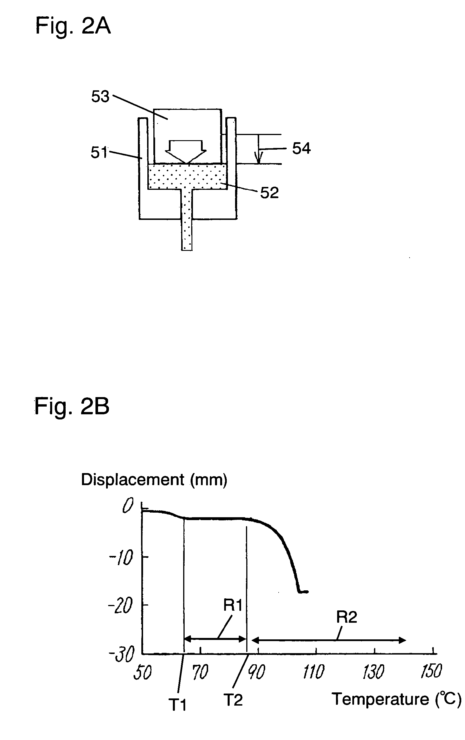
[0087] Laminated body 81 was then put into a vacuum hot pressing machine, heated, and pressurized. FIG. 5 shows temperature profile Tp3 and temperature Tb3 of laminated body 81 at this moment. A temperature of laminated body 81 was maintained at 70° C. within resin softening range R1 for 10 minutes, compressed at 5 MPa, and then cooled to a temperature not higher than 50° C. The temperature-rising rate of temperature profile Tp3 in resin flowing / hardening range R2 was determined to be 5° C. / min.
[0088]FIG. 3 to FIG. 5 show only temperature profiles Tp1, Tp2, and Tp3 and temperatures Tb1, Tb2 and Tb3 of laminated bodies 81 and 181, exclude temperature profiles, pressure profiles, and vacuum pressures in the resin hardenin...
PUM
| Property | Measurement | Unit |
|---|---|---|
| thickness | aaaaa | aaaaa |
| thickness | aaaaa | aaaaa |
| size | aaaaa | aaaaa |
Abstract
Description
Claims
Application Information