Semiconductor device having a roughened surface

a technology of a surface and a surface is applied in the field of semiconductor devices, which can solve the problems of uneven contact resistance between the probe needle and the pad, unstable resistance value, and difficulty in determining the position of the probe, so as to achieve effective removal, improve cleaning performance, and effectively form a chelate complex

Inactive Publication Date: 2007-01-30
RENESAS ELECTRONICS CORP
View PDF19 Cites 16 Cited by
  • Summary
  • Abstract
  • Description
  • Claims
  • Application Information

AI Technical Summary

Benefits of technology

[0018]It is therefore an object of the present invention to provide a semiconductor device and a method for producing the same, by which stabilized resistance is obtained when carrying out a characteristics inspection by bringing a probe into contact with an electrode pad, and the contacting of the probe can be easily recognized through observation by a microscope and the like.
[0019]It is another object of the invention to provide a semiconductor device and a method for producing the same, in which wettability is satisfactory with respect to solder, and solder bumps can be favorably formed on an electrode pad.

Problems solved by technology

In the process of Prior Art 1, when inspecting the characteristics by bringing a probe needle into contact with a bonding pad, there is a problem in that the contact resistance between the probe needle and the pad is uneven.
Since the needle slips, the contact of the pad with the needle is not stabilized, and the contact resistance may change whenever measurement is executed, wherein the value of resistance becomes unstable.
Also, since it is difficult to check the needle mark after the measurement, it becomes difficult to check a shift of the probe in terms of its position.
This is due to a fact that, since the surface of the copper film 17 is flat, it is difficult for scratches by the probe needle to remain thereon.
In this case, there is a concern that the elements may be damaged due to application of a load.
Recently, although a so-called low-k film has been widely used as an interlayer insulating film of semiconductor elements, the hardness of the low-k film is low, and it is liable to be cracked.
Therefore, such a situation arises, in which there is a further concern that the elements may be likely to be damaged due to application of the load.
Conventionally, although copper or a copper alloy of low resistance has been used as a metal that composes the electrode pad, tin is able to easily diffuse these metals and becomes a cause of lowering the reliability of elements.
In the case where such a structure is employed, it is impossible that the contact layer is made thick.
Therefore, with such a structure, it is difficult to apply the technology according to the Prior Art 2, in which unevenness of 0.2 μm or so is provided, to the electrode pad.

Method used


Image

  • Semiconductor device having a roughened surface
  • Semiconductor device having a roughened surface
  • Semiconductor device having a roughened surface

Examples


example 1

[0067]In the example, results of inspection of electrical characteristics using a bonding pad are compared with each other on the basis of the presence of a treatment solution. In the example, a preliminary structure in which an electrode pad composed of a wiring layer and a copper film are provided on a wafer was produced. Evaluation was carried out after the following treatments were carried out on the electrode pad.

[0068]Test Sample a: Untreated.

[0069]Test Sample b: Treated with a blended solution of dilute sulfuric acid and hydrogen peroxide in order to produce unevenness.

[0070]Test Sample c: Treated with a blended solution of dilute sulfuric acid and hydrogen peroxide in order to produce unevenness and also treated with an oxalic acid water solution.

[0071]The ratio of dilute sulfuric acid and hydrogen peroxide in the blended solution was sulfuric acid:hydrogen peroxide:water=1:1:1000 (in terms of cubic volume). And, the oxalic acid water solution was 0.03% by mass.

[0072]With re...

example 2

[0073]A preliminary structure in which an electrode pad composed of a wiring layer and a copper film are provided on a wafer was produced as in Example 1. After the following treatments were carried out on the electrode pad, solder wettability was evaluated.

[0074]Test Sample 1: Untreated.

[0075]Test Sample 2: Treated with an oxalic acid water solution after being treated with a blended solution of dilute sulfuric acid and hydrogen peroxide in order to produce unevenness.

[0076]Test Sample 3: Treated with an oxalic acid water solution after being treated with a blended solution of dilute sulfuric acid and hydrogen peroxide in order to produce unevenness, and next, anticorrosive treatment was conducted on the surface of the electrode pad by an anticorrosive agent.

[0077]The ratio of dilute sulfuric acid and hydrogen peroxide in the blended solution was sulfuric acid:hydrogen peroxide:water=1:1:1000 (in terms of cubic volume). And, the oxalic acid water solution was 0.03% by mass. A benzo...

example 3

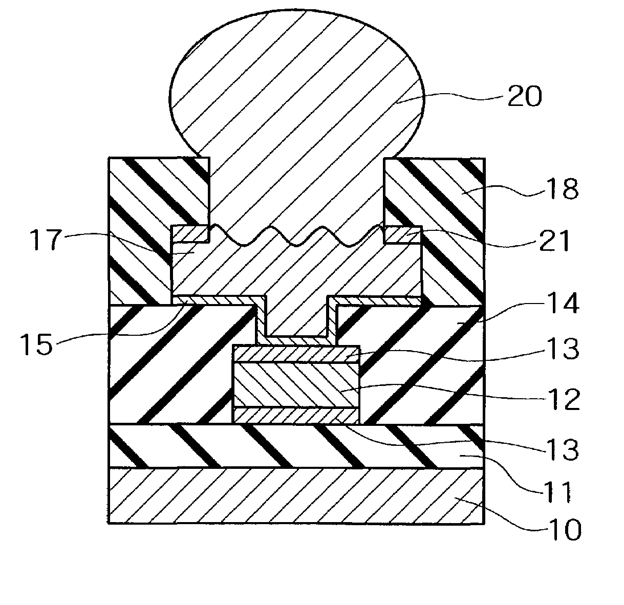
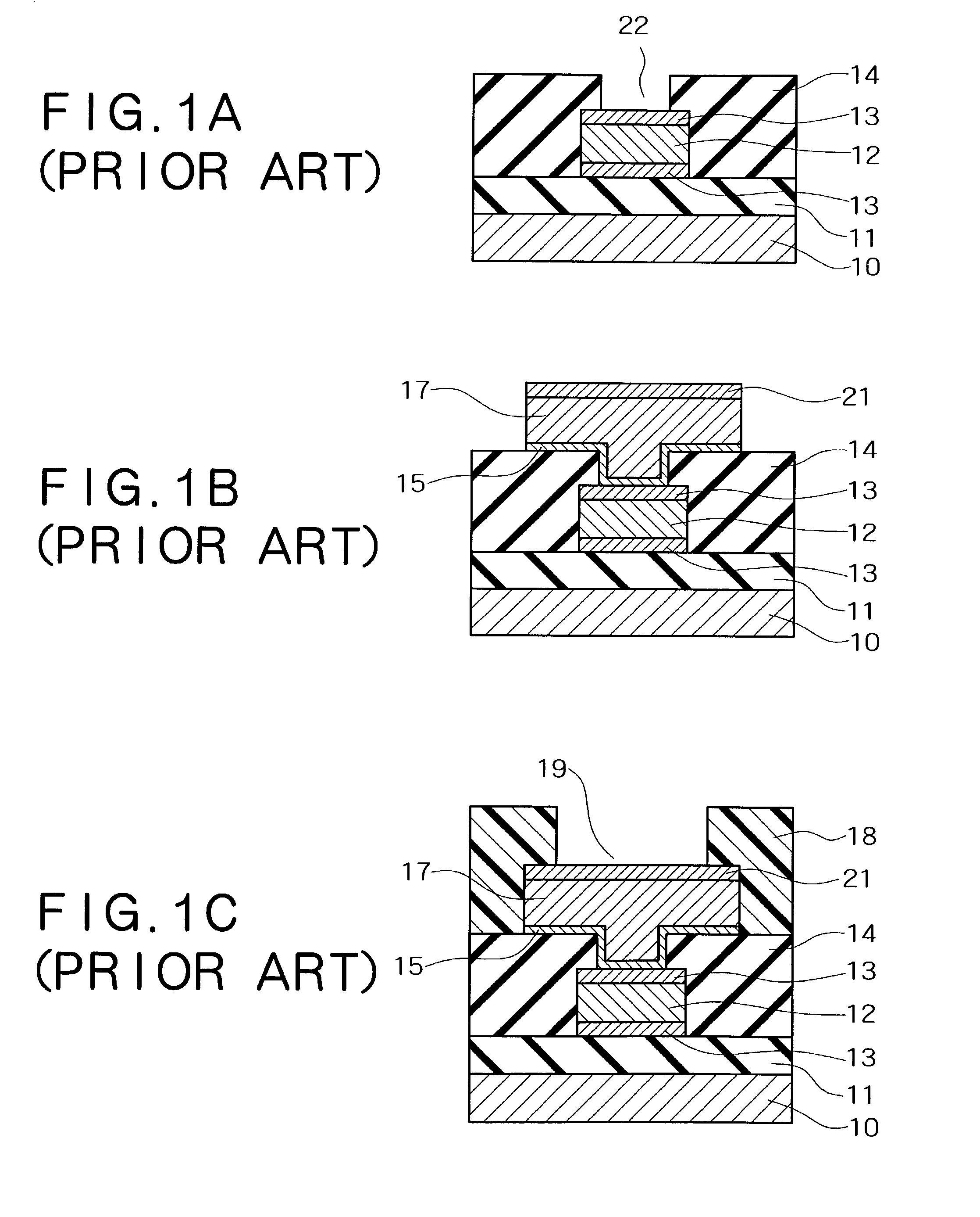
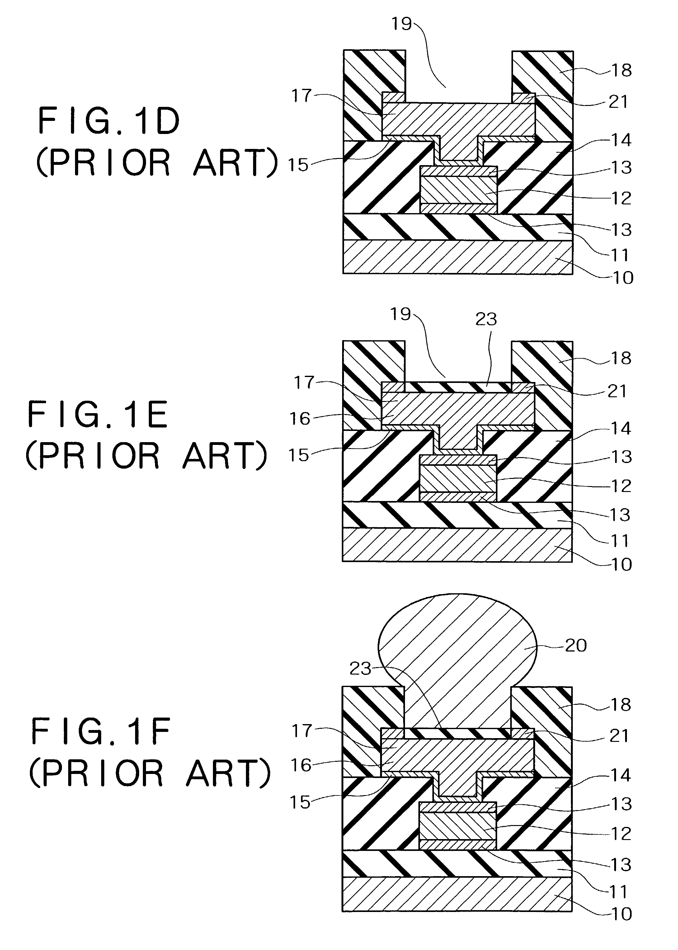
[0079]In the example, processes that are similar to those in FIG. 1A through FIG. 1F and FIG. 2A through FIG. 2D were conducted. At that time, test samples were produced by varying the methods for treatment of the electrode pad surface, and visual recognition of the traces of the probe needle and stability of the contact resistance were evaluated when carrying out the characteristics inspection. The surface treatments of the electrode pad in the respective test samples were as follows:

[0080]Test Sample a: Hydrogen peroxide water treatment was conducted.

[0081]Test Sample b: After hydrogen peroxide water treatment was conducted, a treatment using a blended solution of dilute sulfuric acid and hydrogen peroxide was carried out in order to produce unevenness.

[0082]Test Sample c: After hydrogen peroxide water etching was conducted, a treatment using a blended solution of dilute sulfuric acid and hydrogen peroxide was carried out in order to produce unevenness. Next, still further treatme...


PUM

PropertyMeasurementUnit
surface roughness Raaaaaaaaaaa
thicknessaaaaaaaaaa
surface roughness Raaaaaaaaaaa

Abstract

An oxide film formed on the surface of copper film of an electrode pad is cleaned by oxalic acid after unevenness is formed on the surface of copper film by treating the surface with organic acid. Thereby, stable resistance is obtained when carrying out a characteristic inspection by bringing a probe into contact with the electrode pad, and it is easily recognized by observation through a microscope that the probe is brought into contact with the electrode pad. In addition, wettability with respect to solder is satisfactory, and it is possible to favorably form a solder bump on the electrode pad.

Description

BACKGROUND OF THE INVENTION[0001]1. Technical Field of the Invention[0002]The present invention relates to a semiconductor device having an electrode pad for inspection and a method for producing the same.[0003]2. Description of the Related Art[0004]When inspecting electrical characteristics of a semiconductor device formed on a semiconductor wafer, such a method has been generally employed, by which an inspection is carried out in such a state where an electrode pad for inspection is formed on a device to be inspected, and an inspection probe is brought into contact with the electrode pad. Hereinafter, a description is given of an example (hereinafter called Prior Art 1) for producing a semiconductor device on which an electrode pad for inspection is formed.[0005]FIG. 1A through FIG. 1F are sectional views showing a prior art method for producing a semiconductor device in order of steps. As shown in FIG. 1A, a multilayer film 11 in which a wiring layer and an interlayer insulating ...

Claims


Application Information

Patent Timeline
Patent Type & Authority Patents(United States)
IPC IPC(8): H01L23/48H01L23/52H01L29/40H01L21/66H01L21/306H01L21/3205H01L23/485
CPCH01L24/03H01L24/05H01L2924/0002H01L24/11H01L24/13H01L2224/03019H01L2224/035H01L2224/0381H01L2224/05073H01L2224/05082H01L2224/05155H01L2224/05166H01L2224/05557H01L2224/05561H01L2224/05567H01L2224/05647H01L2924/01004H01L2924/01005H01L2924/01006H01L2924/01013H01L2924/01014H01L2924/01022H01L2924/01028H01L2924/01029H01L2924/01039H01L2924/0105H01L2924/01073H01L2924/01074H01L2924/01075H01L2924/01078H01L2924/01082H01L2924/01088H01L2924/014H01L2924/14H01L2224/0401H01L2924/01033H01L2924/01023H01L2924/01019H01L2224/05552
Inventor TOMIMORI, HIROAKIAOKI, HIDEMITSUMIKAGI, KAORUFURUYA, AKIRATAO, TETSUYA
Owner RENESAS ELECTRONICS CORP
Why Eureka
Try Eureka