Mounting structure mounting substrate, electro-optical device, and electronic apparatus

Active Publication Date: 2006-03-30
BOE TECH GRP CO LTD
View PDF5 Cites 20 Cited by
  • Summary
  • Abstract
  • Description
  • Claims
  • Application Information

AI Technical Summary

Benefits of technology

[0006] An advantage of the invention is that it provides a mounting structure that can further reduce an electrical adhesion area of two substrates and can easily perform an inspection for a positional deviation between connection terminals provided on two substrates, a mounting substrate, an electro-optical device, and an electronic apparatus using such an electro-optical device.
[0007] According to a first aspect of the invention, a mounting structure includes a first substrate that has a first surface and a second surface, a plurality of first connection terminals that are disposed on the first surface in a first direction, a plurality of second connection terminals that are disposed on the first surface in a second direction perpendicular to the first direction and that are disposed at predetermined gaps from the first connection terminals, a plurality of connection wiring lines that are disposed on the second surface, each having first portions that overlap the first and second connection terminals in plan view and a second portion that is formed to have a width narrower than those of the first and second connection terminals in the first direction, a plurality of through holes that pass through the first substrate so as to correspondingly connect the second connection terminals to the connection wiring lines, and a second substrate that has a plurality of third connection terminals being connected to the first and second connection terminals and correspondingly overlapping the first and second connection terminals in plan view.
[0008] According to such a configuration, the first and second connection terminals are provided in the second direction, not in a zigzag shape, and the connection wiring line is provided to overlap the first and second connection terminals. Further, the second connection terminals are electrically connected to the connection wiring lines. Therefore, a conductive pattern electrically connected to the first connection terminals can be provided on the first surface and a conductive pattern electrically connected to, the second connection terminals can be provided on the second surface. That is, the conductive patterns can be provided on separate surfaces. Therefore, more connection terminals can be provided in the same area, as compared with the case in which the connection terminals are provided in the zigzag shape. Specifically, in a case in which a same number of connection terminals are provided, it is possible to reduce the connection area of the first substrate and the second substrate. Further, on the first substrate, the connection wiring line overlaps the first and second connection terminals in plan view, and at least a portion (the second portion) of the connection wiring line has a width narrower than that of each of the first and second connection terminals. Therefore, after the first substrate and the second substrate are connected to each other, an inspection for a positional deviation of both substrates, that is, an inspection for connection defects of the first and second connection terminals and the third connection terminal, can be easily performed. For example, it is assumed that the first substrate and the second substrate have higher transmittance than the first connection terminal, the second connection terminal, the third connection terminal and the connection wiring line. More specifically, it is assumed that the first substrate and the second substrate have light transmissive properties, while the first connection terminal, the second connection terminal, the third connection terminal, and the connection wiring line have light-shielding properties. In this case, the inspection for a positional deviation can be performed by irradiating light onto the mounting structure from one side thereof and observing transmitted light from the other side thereof. If doing so, it can be observed that light passes through in a region where only the first substrate exists, a region where only the second substrate exists, or a region where only the first substrate and the second substrate overlap. On the other hand, it can be observed that light is shielded in a region where at least one of the first, second and third connection terminals and the connection wiring line exists. Then, the pattern shape of the light shielding region can be visually recognized through brightness of the light transmission region and the light shielding region. Then, only in a case in which the patte

Problems solved by technology

However, in the liquid crystal device having the above-described configuration, the connection terminals are arranged in the zigzag shape in a plurality of lines, and thus the adhesion area region of the flexible wiring board and the circuit board can be reduced, as compared with the case in which the connection terminals are arranged in a line, but there is a problem in that the adhesion area region cannot be sufficiently ensured.
Further, the inspection for a positional deviation of the connection terminals on the flexible wiring board and the connection terminals of the circuit board cannot be easily performed.
In addition, whether or not there are connection defects of the flexible wiring board and the circuit board needs be checked with the naked eye or the like.
For this reason, there is a problem in that work efficiency may be degraded.
Further, in a case in which a light transmissive property is bad since the second substrate is of a four-layered substrate structure or the like, the inspection for a positional deviation can be performed by reflection.
Further, in a case in which a light transmissive property is bad since the second substrate is of a four-layered substrat

Method used


Image

  • Mounting structure mounting substrate, electro-optical device, and electronic apparatus
  • Mounting structure mounting substrate, electro-optical device, and electronic apparatus
  • Mounting structure mounting substrate, electro-optical device, and electronic apparatus

Examples


Embodiment Construction

[0043] Hereinafter, embodiments of the invention will be described with reference to the drawings. Moreover, in the embodiment described below, a liquid crystal device will be used as an electro-optical device. Specifically, a simple matrix-type liquid crystal device of a COG method is described, but an active matrix-type liquid crystal device of a TFT method or TFD method may be used. Further, in the drawings, the scale of each part or the number of parts has been adjusted in order to have a recognizable size.

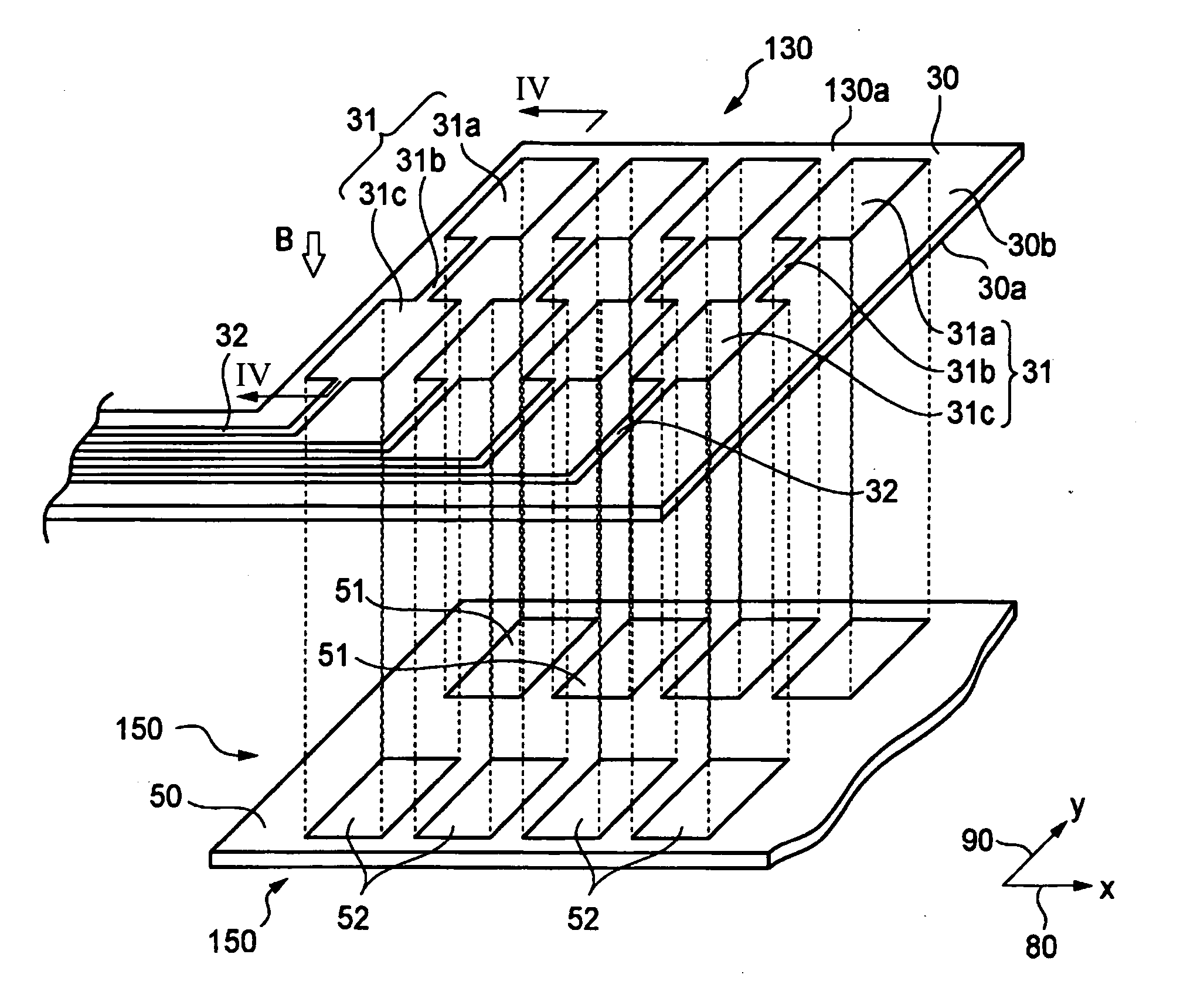
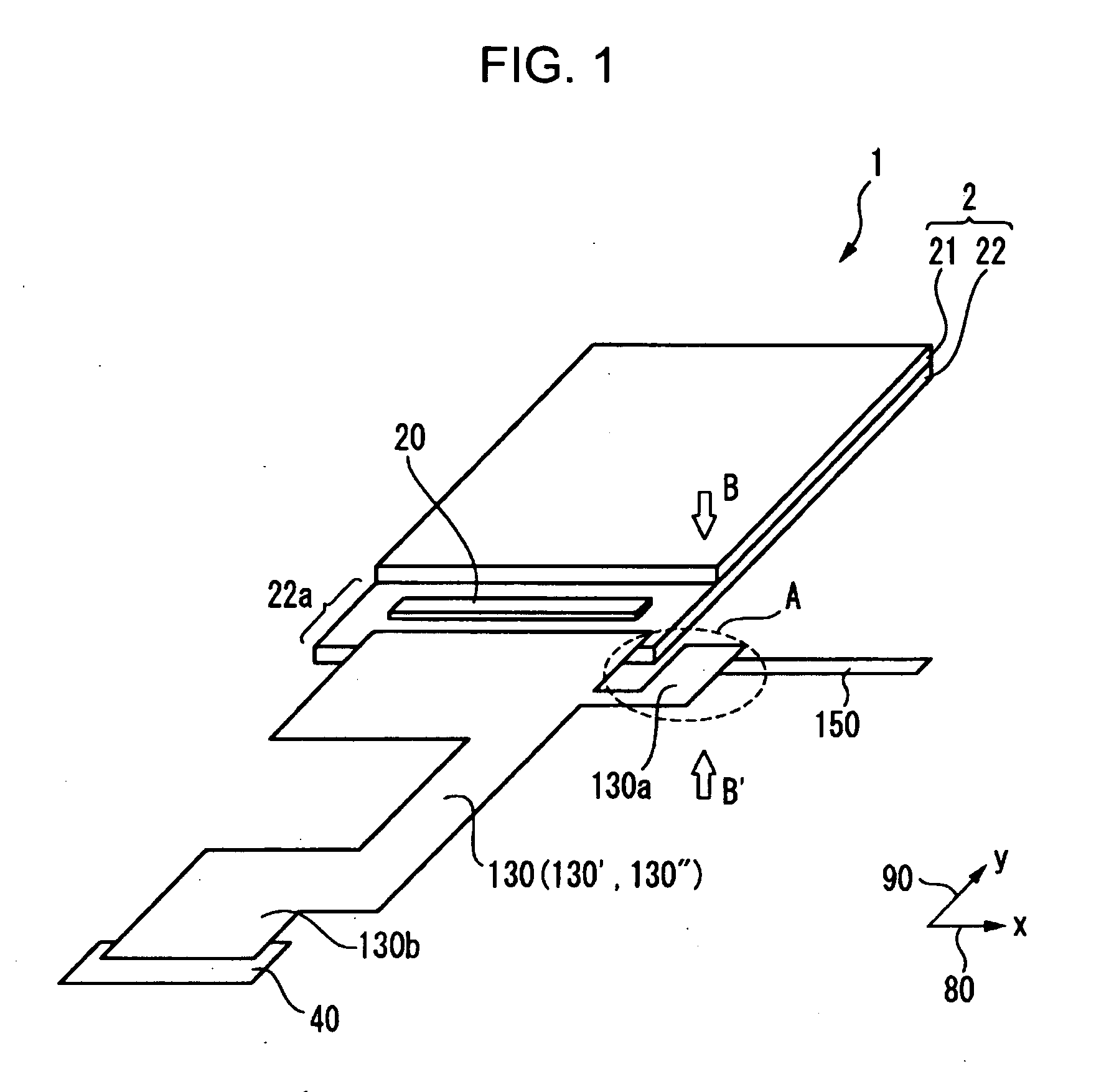
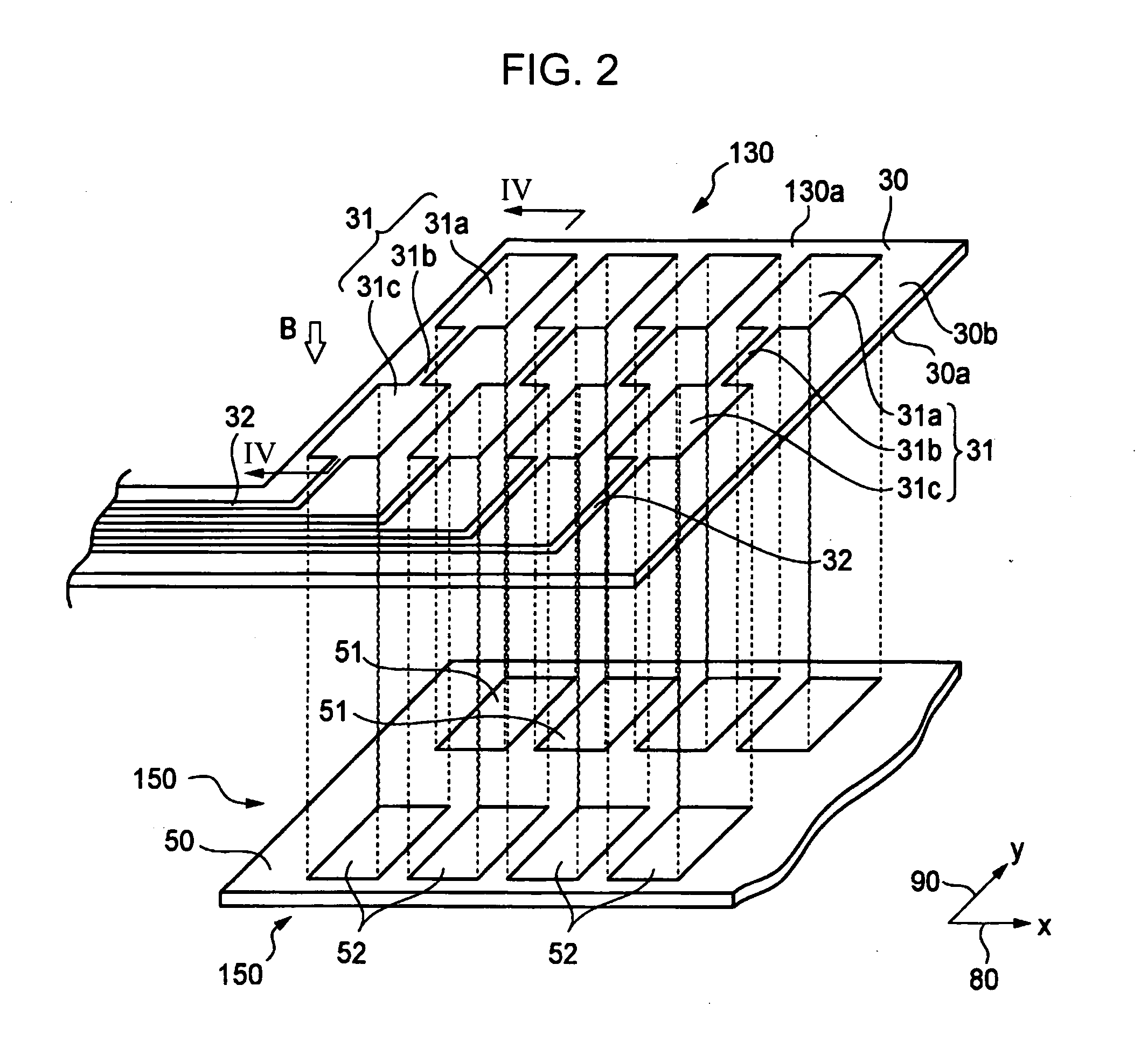
[0044]FIG. 1 is a schematic perspective view of a liquid crystal device, which is an example of an electro-optical device having a mounting structure according to an embodiment of the invention. FIG. 2 is an exploded perspective view of a region which is encircled by an ellipse A of FIG. 1 in a magnified scale. Further, in FIG. 2, an ACF (Anisotropic Conductive Film) serving as a conductive member which electrically connects a flexible wiring board to a rigid substrate is omi...


PUM


Abstract

A mounting structure includes a first substrate that has a first surface and a second surface, a plurality of first connection terminals that are disposed on the first surface in a first direction, a plurality of second connection terminals that are disposed on the first surface in a second direction perpendicular to the first direction and that are disposed at predetermined gaps from the first connection terminals, a plurality of connection wiring lines that are disposed on the second surface, each having first portions that overlap the first and second connection terminals in plan view and a second portion that is formed to have a width narrower than those of the first and second connection terminals in the first direction, a plurality of through holes that pass through the first substrate so as to correspondingly connect the second connection terminals to the connection wiring lines, and a second substrate that has a plurality of third connection terminals correspondingly connected to the first and second connection terminals and correspondingly overlap the first and second connection terminals in plan view.

Description

BACKGROUND OF THE INVENTION [0001] 1. Technical Field [0002] The present invention relates to a mounting structure which has two substrates electrically connected to each other, to a mounting substrate, to an electro-optical device, and to an electronic apparatus using such an electro-optical device. [0003] 2. Related Art [0004] An electro-optical device, for example, a liquid crystal device of a COG (Chip on Glass) method, includes a liquid crystal panel in which liquid crystal is sealed between a pair of substrates, a semiconductor element that is mounted on a substrate of the liquid crystal panel, a flexible wiring board that is electrically connected to the semiconductor element, and a circuit board that supplies signals to the liquid crystal panel via the flexible wiring board and the semiconductor element. In this case, connection terminals, which are respectively provided on the flexible wiring board and the circuit board as electrode patterns, are electrically connected to e...

Claims


Application Information

Patent Timeline
IPC IPC(8): H05K7/06
CPCG02F1/13452H05K1/117H05K3/323H05K2201/09727H05K2201/09409H05K2201/09481H05K3/361G02F1/1345
Inventor YUMOTO, MASANORIHIRANO, YOSHIHISA
Owner BOE TECH GRP CO LTD
Why Eureka
Try Eureka