Display element drive circuit and display apparatus

a drive circuit and display element technology, applied in the direction of instruments, semiconductor devices, computing, etc., can solve the problems of deterioration of display image quality, large dcp of the display element drive circuit, and irregular operation characteristics, so as to suppress the occurrence of delay of write operation, improve display image quality, and improve display image quality

Active Publication Date: 2006-03-30
SOLAS OLED LTD
View PDF12 Cites 40 Cited by
  • Summary
  • Abstract
  • Description
  • Claims
  • Application Information

AI Technical Summary

Benefits of technology

[0025] In a display apparatus provided with a display panel which has a display element and a display element drive circuit which drives the display element in a display pixel, the present invention has an advantage of improving a display image quality while suppressing occurrence of a delay of a write operation, insufficient writing, deterioration of luminance characteristics and the like due to a parasitic capacitance or a retention volume caused by a plurality of transistors constituting the display element drive circuit.

Problems solved by technology

Further, when each display pixel is miniaturized in order to achieve high definition, irregularities in operation characteristics (a current between the source and the drain or the like) of both transistors Tr111 and Tr112 constituting the display element drive circuit DCp become large.
Therefore, an appropriate gradation control cannot be performed, and irregularities are produced in light emission characteristics of each display pixel, thereby resulting in deterioration of a display image quality.
However, the display element drive circuit adopting the current application mode has the following problems.
Therefore, an operation is delayed or insufficient writing occurs, whereby the display element cannot perform the light emitting operation with an appropriate luminance gradation corresponding to display data in some cases.
Furthermore, various kinds of capacitance components existing in the display element drive circuit of the display pixel have the following problem.

Method used


Image

  • Display element drive circuit and display apparatus
  • Display element drive circuit and display apparatus
  • Display element drive circuit and display apparatus

Examples


first embodiment

of Display Element Drive Circuit

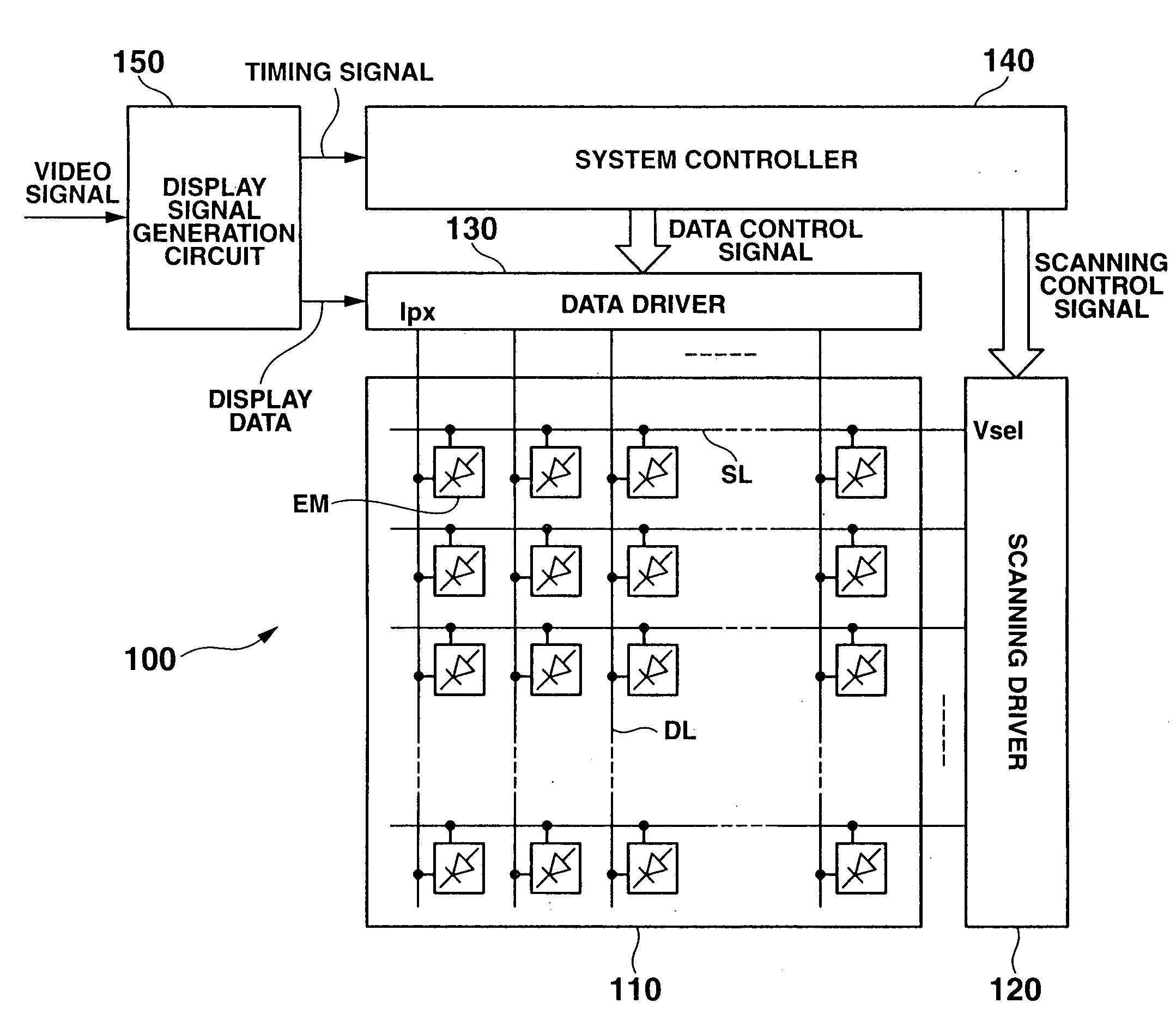
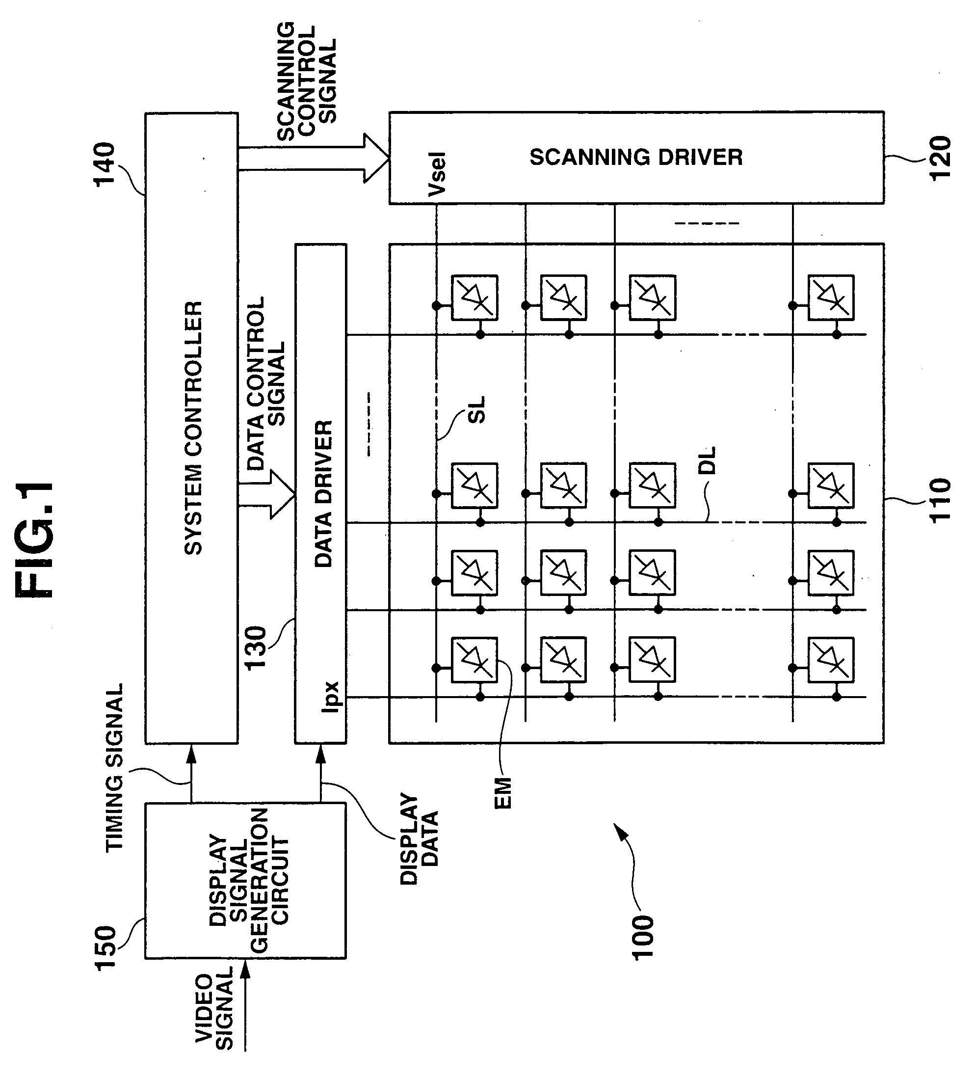
[0164]FIG. 8 is a circuit configuration view showing a first embodiment of the display element drive circuit according to the present invention. FIGS. 9A and 9B are schematic structural views showing a structural example of an element configuration of a thin film transistor applied to the display element drive circuit according to this embodiment.

[0165] In FIG. 8, like reference numerals denote circuit configurations equivalent to those in the display element drive circuit, thereby simplifying the explanation. Moreover, in FIGS. 9A and 9B, hatching is provided to a drain electrode, a data line and a source electrode in order to clarify the drawings for the convenience's sake.

[0166] As shown in FIG. 8, in a circuit configuration equivalent to the display element drive circuit DC depicted in FIG. 3, a display element drive circuit DCA according to this embodiment has a structure in which, of parasitic capacitances formed in a write control thin film t...

second embodiment

of Display Element Drive Circuit

[0200]FIG. 13 is a circuit configuration view showing a second embodiment of the display element drive circuit according to the present invention.

[0201]FIG. 14 is a characteristic view showing a relationship between a parasitic capacitance of a light emission control thin film transistor and an output current (a driving current) with respect to a write current (a gradation signal current).

[0202] Here, like reference numerals denote circuit configurations equal to those in the first embodiment, thereby simplifying the explanation.

[0203] As shown in FIG. 13, in the same circuit configuration as the display element drive circuit DC depicted in FIG. 3, a display element drive circuit DCB according to this embodiment has a structure in which, of parasitic capacitances formed in a light emission control thin film transistor or third transistor Tr13 in which one end side of a current path (a source electrode side) is connected with an organic EL element (...

third embodiment

of Display Element Drive Circuit

[0213]FIG. 15 is a circuit configuration view showing a third embodiment of the display element drive circuit according to the present invention.

[0214] Here, like reference numerals denote the same circuit configurations as those in the foregoing embodiments, thereby simplifying the explanation.

[0215] As shown in FIG. 15, in the same circuit configuration as the display element drive circuit DC depicted in FIG. 3, a display element drive circuit DCC according to this embodiment has a structure in which, of parasitic capacitances formed in a write control thin film transistor or first transistor Tr11 in which one end side of a current path (a source electrode side) is connected with a gate terminal (a contact point N11) of a third thin film transistor Tr13, the other end side (a drain electrode side) is connected with a power supply line VL and a control terminal (a gate electrode) is connected with a scanning line SL, a parasitic capacitance Cgd1 be...


PUM


Abstract

A display element drive circuit includes a first circuit which holds as a voltage component electric charges based on a gradation signal corresponding to display data, a second circuit which supplies the gradation signal to the electric charge holding circuit at a timing of application of a selection signal, current control type display elements, and a third circuit which generates a driving current based on the voltage component held in the first circuit and supplies the generated driving current to the display element. One of the second and third circuits includes at least one field effect transistor. The field effect transistor includes gate, electrode and drain electrodes, and a source-side parasitic capacitance formed between the gate and source electrodes and a drain-side parasitic capacitance formed between the gate and drain electrodes of the field effect transistor have different capacitance values.

Description

CROSS-REFERENCE TO RELATED APPLICATIONS [0001] This application is based upon and claims the benefit of priority from prior Japanese Patent Application No. 2004-279268, filed Sep. 27, 2004, the entire contents of which are incorporated herein by reference. BACKGROUND OF THE INVENTION [0002] 1. Field of the Invention [0003] The present invention relates to a display element drive circuit and a display apparatus comprising the display element drive circuit, and more particularly to a display element drive circuit which is provided in each display pixel in a display panel and drives a display element based on a driving current corresponding to a gradation signal and to a display apparatus comprising a display panel in which display pixels each having the display element drive circuit are two-dimensionally arranged. [0004] 2. Description of the Related Art [0005] There has been conventionally known a self-luminous type display (a display apparatus) including a display panel in which dis...

Claims


Application Information

Patent Timeline
Patent Type & Authority Applications(United States)
IPC IPC(8): G09G5/10
CPCG09G3/325G09G3/3283G09G2300/0417G09G2300/0842G09G2300/0847H01L27/124G09G2320/0219H01L29/41733H01L29/42384H01L29/78696G09G2300/0866
Inventor YAMAGUCHI, IKUHIROTAKEI, MANABU
Owner SOLAS OLED LTD
Why Eureka
Try Eureka