Microelectromechanical modulation device and microelectromechanical modulation device array, and image forming apparatus

a microelectromechanical and modulation device technology, applied in the direction of optics, instruments, optical elements, etc., can solve the problems of affecting the speed of switching operation, and taking time to stop the oscillation, so as to reduce the driving cycle, active reduction of the oscillation of the movable portion, and the effect of reducing the time of anon/o

Inactive Publication Date: 2006-03-30
FUJIFILM HLDG CORP +1
View PDF3 Cites 22 Cited by
  • Summary
  • Abstract
  • Description
  • Claims
  • Application Information

AI Technical Summary

Benefits of technology

[0058] This image forming apparatus of one embodiment of the invention has one of the modulation device arrays according to any one of (10) to (12) as a primary part. Thus, the oscillation of the movable portion can be actively reduced. The driving cycle can be reduced, as compared with a related art apparatus. This enables high-speed exposure of a photosensitive material, and display in a higher-pixel projector. Further, an image forming apparatus (or an exposure apparatus) adapted to perform gradation control by switching on / off of exposing light can reduce anon / off time. Thus, higher gradation can be realized.
[0059] The microelectromechanical modulation device according to the invention has a plurality of drive sources operative to apply a physical action force to the movable portion. When the movable portion is displacement-driven in a first direction, a physical action force for suppressing the oscillation of the movable portion is applied to the movable portion by the drive sources while the movable portion is transited in the first direction. Thus, a physical attraction force is exerted in a direction opposite to the direction of transition of the movable portion. The oscillation of the movable portion, which is caused when the movable portion is put into contact with a stopping member, can be actively reduced. Consequently, the speeding-up of a switching operation of the microelectromechanical modulation device can be achieved.
[0060] In accordance with the microelectromechanical modulation device array according to the invention, after the movable portion reaches the final displacement position, the oscillation of the movable portion is suppressed. Therefore, an oscillation stopping time can be eliminated or can be considerably reduced. The writing of address voltages can be performed without necessity for waiting for the stop of the oscillation. Consequently, the speeding-up of a switching operation can be achieved by reducing a driving cycle.
[0061] The image forming apparatus according to the invention has a light source, the microelectromechanical modulation device array according to any one of (10) to (12), an illuminating optical system adapted to irradiating light, which is outputted from the light source, onto the the microelectromechanical modulation device array, and a projection optical system adapted to project light, which is outputted from the microelectromechanical modulation device array, onto an image forming surface. Thus, as compared with a related art apparatus, the length of time required to perform a switching operation can be reduced. This enables high-speed exposure of a photosensitive material, and display in a higher-pixel projector.

Problems solved by technology

Consequently, it takes time to stop the oscillation.
Such oscillation and overshoots hinder the speeding-up of a switching operation of the microelectromechanical modulation device.
Consequently, this device has a disadvantage in that this device is poor in diversity of oscillation control methods.
For instance, when the movable portion is attracted and displaced to the substrate, an opposite damping force cannot be applied to the movable portion.
That is, the oscillation thereof cannot be actively reduced.
Consequently, this optical path switching device has a disadvantage in that this device is poor in diversity of oscillation control methods.
Thus, similarly to the microelectromechanical grating device, this optical path switching device cannot actively reduce the oscillation of the movable portion.
Thus, this control method cannot actively reduce the oscillation of the movable portion.

Method used


Image

  • Microelectromechanical modulation device and microelectromechanical modulation device array, and image forming apparatus
  • Microelectromechanical modulation device and microelectromechanical modulation device array, and image forming apparatus
  • Microelectromechanical modulation device and microelectromechanical modulation device array, and image forming apparatus

Examples


first embodiment

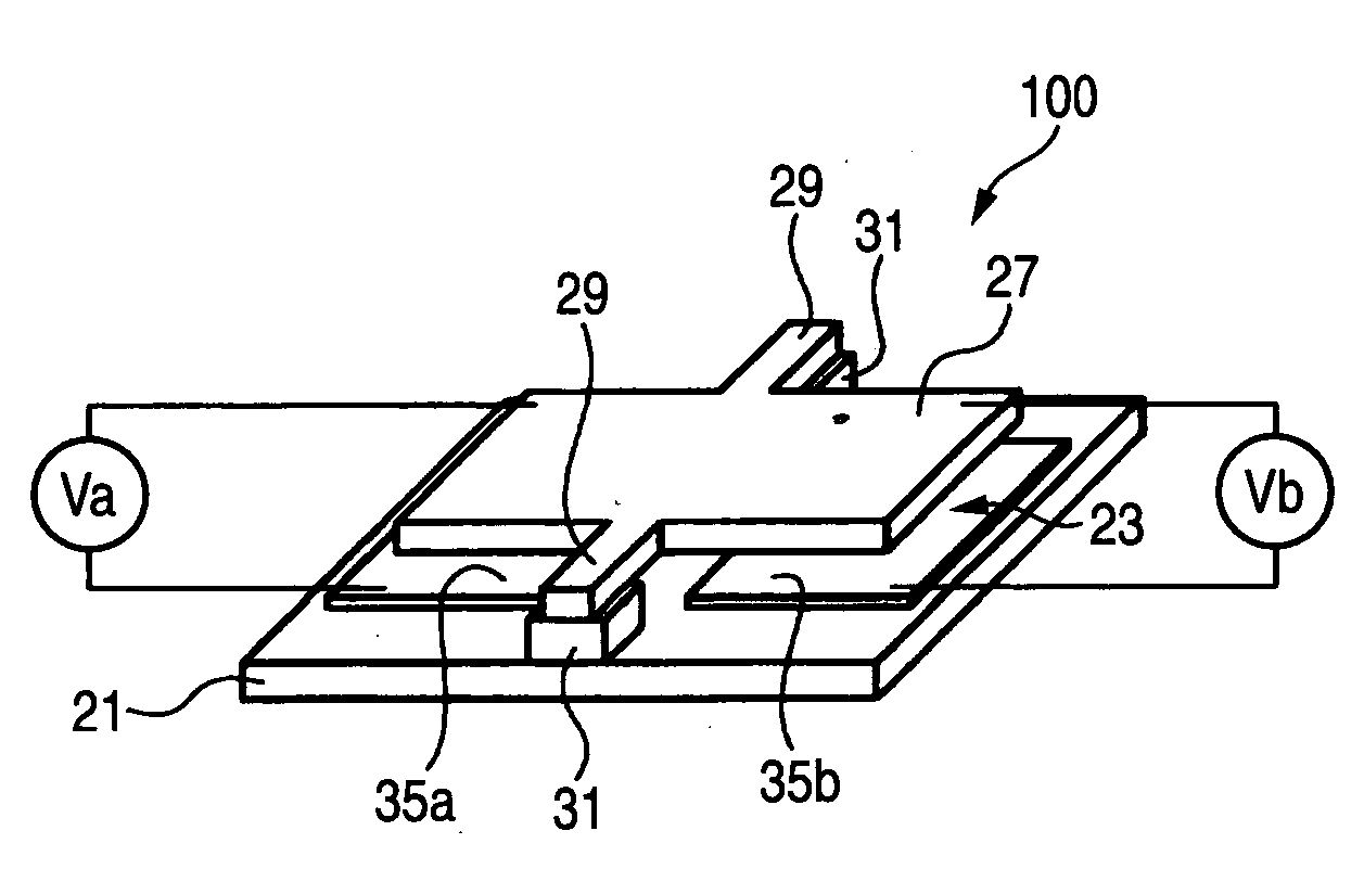
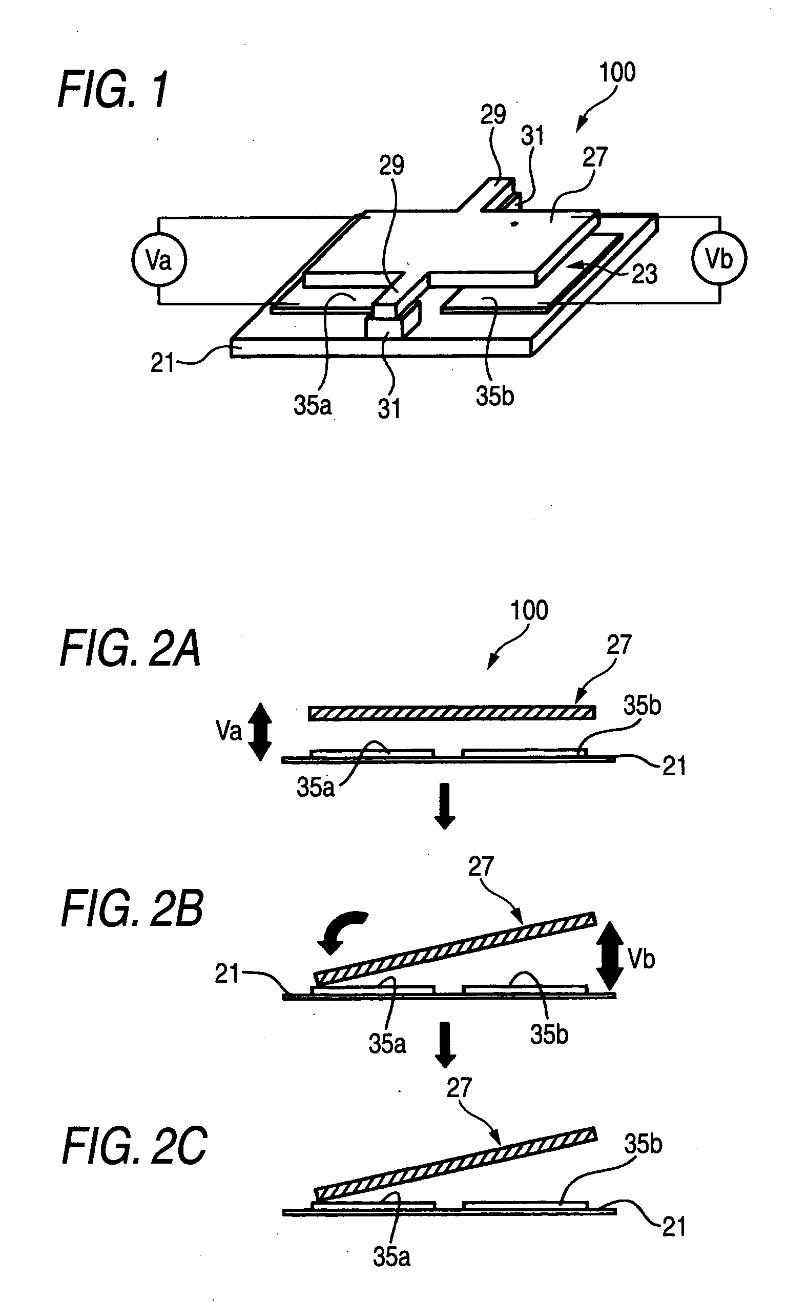
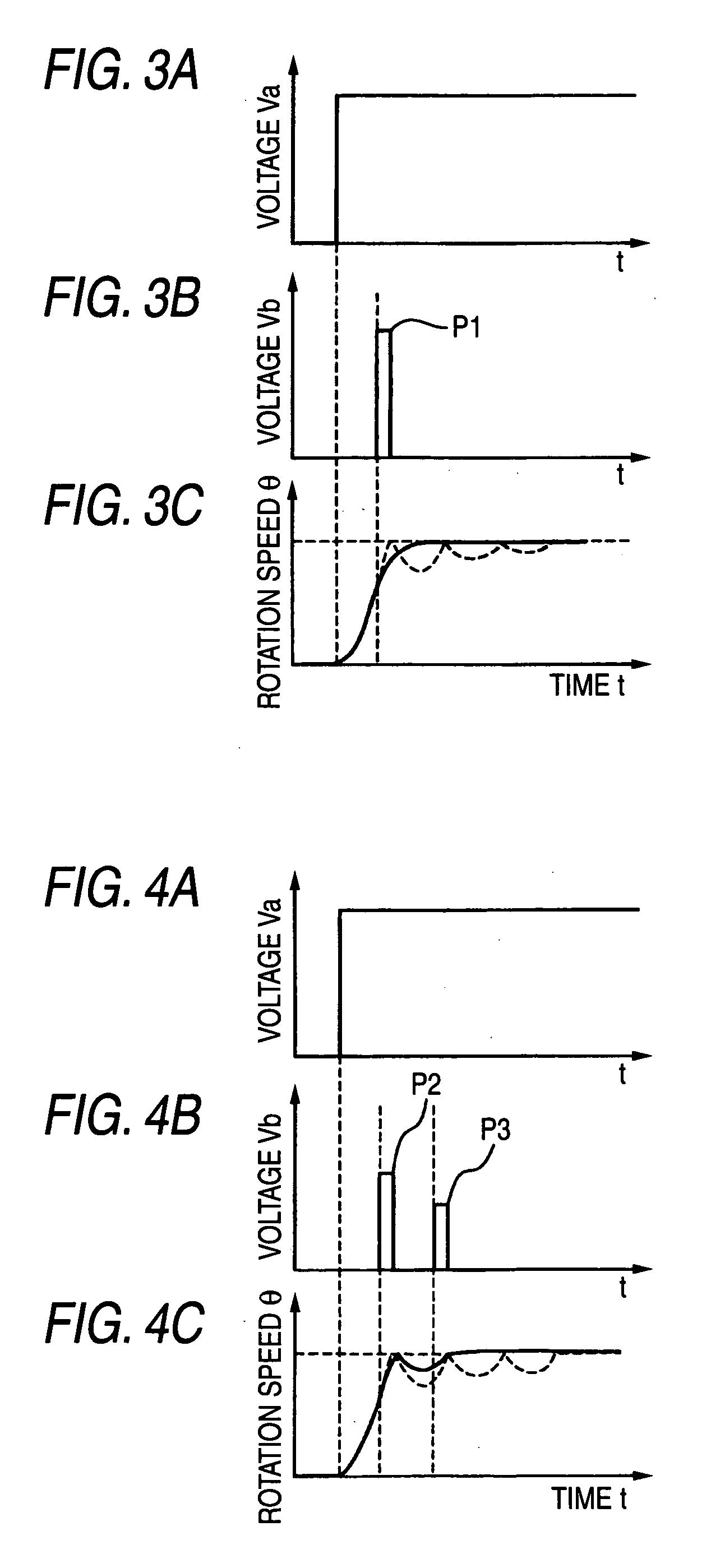
[0087]FIG. 1 is a conceptual view illustrating a microelectromechanical modulation device according to the invention. FIGS. 2A to 2C are operation explanatory views illustrating a damping process of the microelectromechanical modulation device shown in FIG. 1. FIGS. 3A to 3C are explanatory views illustrating a behavior of a movable portion to which a pulse waveform is applied.

[0088] The microelectromechanical modulation device (hereunder also referred to simply as a “modulation device”) 100 according to this embodiment includes a substrate 21, a small-piece-like movable portion disposed in parallel to the substrate 21 through a gap 23, hinges 29, 29 respectively extended from both edge parts of the movable portion 27, and spacers 31, 31 supporting the movable portion 27 on the substrate 21 through these hinges 29, 29, as fundamental components. By this configuration, the movable part is capable of being rotated and transited by the distortion of the hinges 29, 29.

[0089] When the m...

second embodiment

[0139] Next, the microelectromechanical device according to the invention is described hereinbelow.

[0140]FIG. 14 is a conceptual view illustrating the second embodiment of the microelectromechanical modulation device according to the invention.

[0141] A modulation device 200 according to this embodiment is configured so that two or more physical action forces can be set corresponding to the direction of transition of the movable portion 27. That is, a set of a main first address electrode 35a1, and an auxiliary first address electrode 35a2, and another set of a main second address electrode 35a1 and an auxiliary second address electrode 35b2 are provided on both sides of the hinges 29, 29 on the central part of the top surface of the substrate 21. A driving voltage Val is applied between the main first address electrode 35a1 and the movable portion 27, while a driving voltage Va2 is applied between the auxiliary first address electrode 35a2 and the movable portion 27. Further, an os...

third embodiment

[0144] Next, the microelectromechanical device according to the invention is described hereinbelow.

[0145]FIG. 15 is a conceptual view illustrating a third embodiment of the microelectromechanical modulation device according to the invention.

[0146] A modulation device 300 according to this embodiment is configured so that one of ends of a movable portion 41 is supported by and is fixed to the substrate 21 through the hinges 29, 29 and spacers 31, 31. That is, the movable portion 41 is configured like a cantilever, so that the other end of the movable portion 41 is a free end. Further, a first address electrode 35a facing the free end of the movable portion 41 is provided on the substrate 21. A second address electrode 35b to be formed on an opposed substrate (not shown) is provided on the side opposite to the first address electrode 35a so that the movable portion 41 is sandwiched between the first address electrode 35a and the second address electrode 35b.

[0147] Even in the modula...


PUM


Abstract

A microelectromechanical modulation device comprising: a movable portion, which is supported to be elastically and bi-directionally displaced and which has a modulation function; and a plurality of driving sources operative to apply a physical action force to said movable portion, wherein when said movable portion is displacement-driven in a first direction, a physical action force for suppressing oscillation of said movable portion is applied to said movable portion in a second direction different from the first direction by said drive sources while said movable portion is transited in the first direction.

Description

[0001] This application is based on Japanese Patent application JP 2004-287975, filed Sep. 30, 2004, the entire content of which is hereby incorporated by reference. This claim for priority benefit is being filed concurrently with the filing of this application. BACKGROUND OF THE INVENTION [0002] 1. Technical Field of the Invention [0003] The present invention relates to a microelectromechanical modulation device which has a movable portion that is bi-directionally displaced, to a microelectromechanical modulation device array, and to an image forming apparatus. More particularly, the present invention relates to improved techniques for damping the movable portion. [0004] 2. Description of the Related Art [0005] In recent years, rapid progress of MEMS (MicroElectroMechanical Systems) technology has resulted in extensive development of a microelectromechanical modulation device that electrically displaces or moves a microstructure having a size in the order of micrometers. This micro...

Claims


Application Information

Patent Timeline
Patent Type & Authority Applications(United States)
IPC IPC(8): G02B26/00
CPCG02B26/0841
Inventor OGIKUBO, SHINYANAKAMURA, HIROCHIKA
Owner FUJIFILM HLDG CORP
Why Eureka
Try Eureka