Thin film transistor array substrate and manufacturing method thereof

a technology of thin film transistors and manufacturing methods, applied in semiconductor devices, radio frequency controlled devices, instruments, etc., can solve the problems of unsuitable for large-scale liquid crystal display panels, less desirable paving the way to develop display devices,

Inactive Publication Date: 2006-04-06
CHUNGHWA PICTURE TUBES LTD
View PDF5 Cites 13 Cited by
  • Summary
  • Abstract
  • Description
  • Claims
  • Application Information

AI Technical Summary

Benefits of technology

[0009] Accordingly, the present invention is directed to a thin film transistor array substrate and a

Problems solved by technology

However, with the recent campaign for protecting the environmental, its bulkiness, high power consumption and high radiation makes it less desirable paving a way to develop display dev

Method used


Image

  • Thin film transistor array substrate and manufacturing method thereof
  • Thin film transistor array substrate and manufacturing method thereof
  • Thin film transistor array substrate and manufacturing method thereof

Examples


Embodiment Construction

[0022] Reference will now be made in detail to the present preferred embodiments of the invention, examples of which are illustrated in the accompanying drawings. Wherever possible, the same reference numbers are used in the drawings and the description to refer to the same or like parts.

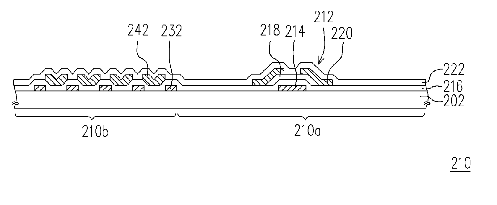
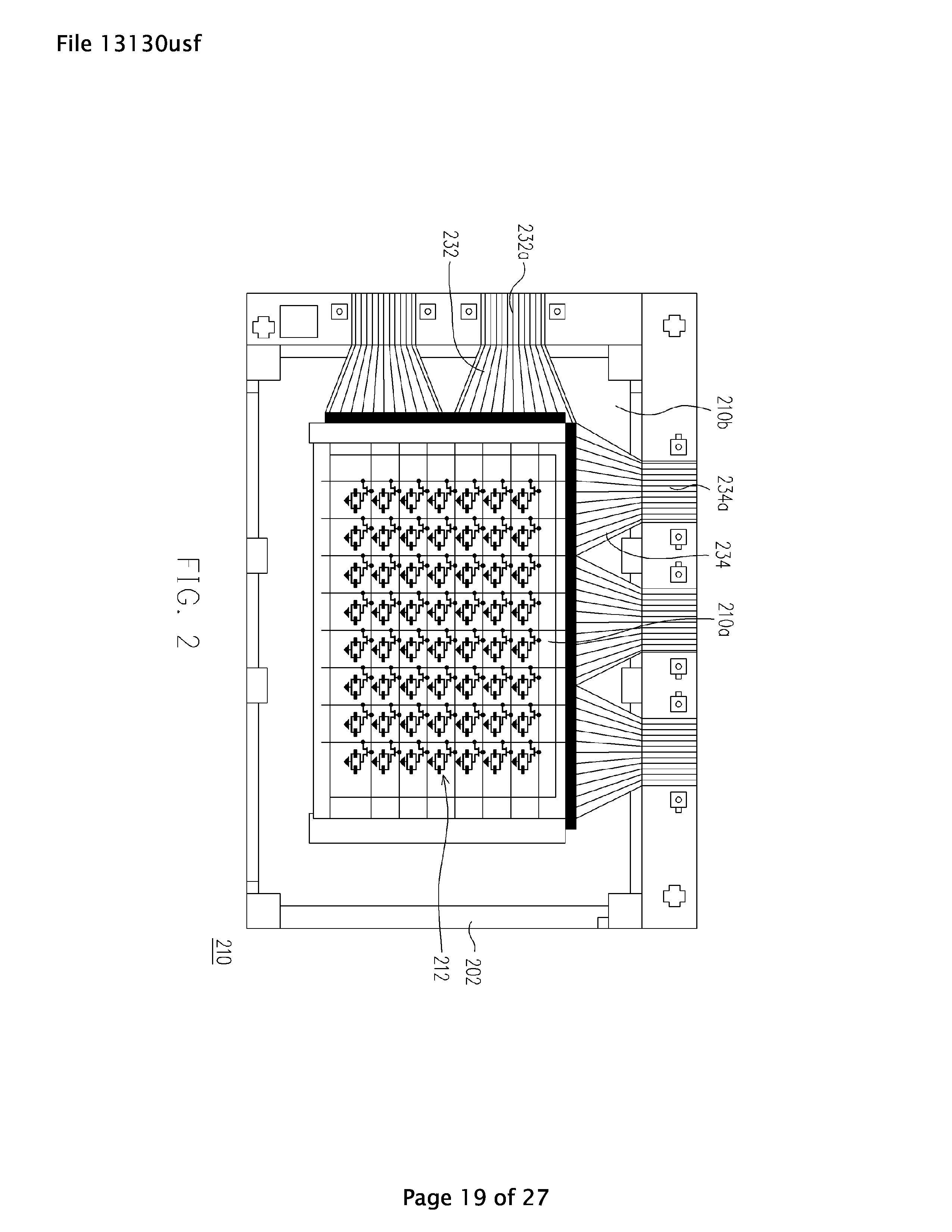
[0023]FIG. 2 is a top view of a thin film transistor array according to an embodiment of the present invention. FIG. 3 is a cross-sectional view showing a local section of a thin film transistor array according to an embodiment of the present invention. As shown in FIG. 2, the thin film transistor array substrate 210 includes a pixel region 210a and a peripheral region 210b surrounding the pixel region 210a. A thin film transistor array 212 comprising a plurality of thin film transistors and a plurality of pixel electrodes (not shown) are disposed on a transparent substrate 202 within the pixel region 210a. A plurality of lead lines such as gate lines 232 or source lines 234 linking with the thin f...


PUM


Abstract

A thin film transistor array substrate and manufacturing method thereof are provided. A shielding layer is formed between lead lines in a peripheral region of the substrate. The shielding layer and a gate layer may be formed simultaneously so that the light leakage between lead lines connected to a source/drain layer is reduced. Alternatively, the shielding layer and the source/drain layer may be formed simultaneously so that the light leakage between lead lines connected to a gate layer is reduced. Furthermore, a common voltage may be applied to the shielding layer so that signal interference between lead lines is reduced. Moreover, in an electrical inspection of the thin film transistor array, any short circuit between the lead lines and the shielding layer can be determined.

Description

BACKGROUND OF THE INVENTION [0001] 1. Field of the Invention [0002] The present invention relates to a display panel and manufacturing method thereof. More particularly, the present invention relates to a thin film transistor array substrate and manufacturing method thereof. [0003] 2. Description of the Related Art [0004] With the increase in computing power and the rapid development of Internet and multimedia technologies, most image data are transmitted in digital format rather than analogue format. To match the life style of modern people, video or image devices have been developed to be small and compact. In the past, conventional cathode ray tubes (CRT) used to be the dominant display devices because their high display quality and a low cost features. However, with the recent campaign for protecting the environmental, its bulkiness, high power consumption and high radiation makes it less desirable paving a way to develop display devices that are small, compact and energy-saving...

Claims


Application Information

Patent Timeline
IPC IPC(8): H01L27/148
CPCG02F1/133509H01L27/124G02F1/1345
Inventor HSU, HAN-TUNGLIU, WEN-HSIUNGHE, CHIEN-KUO
Owner CHUNGHWA PICTURE TUBES LTD
Why Eureka
Try Eureka