Semiconductor package with package-on-package stacking capability and method of manufacturing the same

a technology of semiconductor packaging and stacking capability, applied in the manufacture of printed circuits, basic electric elements, solid-state devices, etc., can solve the problems of significant thermal, electrical and reliability challenges in the semiconductor packaging industry, many manufacturing yield-related deficiencies remain, and shortening between neighboring countries

Inactive Publication Date: 2015-06-04
BRIDGE SEMICON
View PDF13 Cites 33 Cited by
  • Summary
  • Abstract
  • Description
  • Claims
  • Application Information

AI Technical Summary

Benefits of technology

[0013]The method of making a semiconductor package for package-on-package stacking applications according to the present invention has numerous advantages. For instance, forming the chip-on-interposer subassembly before attaching it to the base carrier can ensure the semiconductor device is electrically connected so that any contact pad disconnection problem inherent to micro-via process can be avoided. Inserting the semiconductor device to the through opening by the chip-on-interposer subassembly is particularly advantageous as the shape of the through opening would not be a critical parameter that needs to be tightly controlled. Additionally, the two-step forming of the interconnect substrate for the semiconductor device is beneficial as the interposer can provide primary fan-out routing whereas the buildup circuitry provide further fan-out routing and horizontal interconnections between the upper and the lower packages.

Problems solved by technology

The convergence of mobility, communication, and computing has created significant thermal, electrical and reliability challenges to the semiconductor packaging industry.
Despite numerous package-on-package assemblies reported in the literature, many manufacturing yield-related deficiencies remain.
As a result, the use of the micro-via approach presents a crowding problem which can cause shorting between the neighboring micro-vias.
Another significant drawback arising from the fabrication of the above assemblies is that the embedded chip may dislocate during encapsulation or lamination.
Incomplete metallization of micro-vias due to chip dislocation as described in U.S. Pat. No. 8,501,544 further degrades the quality of the electrical connection, thereby lowering the reliability and production yield of the fabricated assembly.

Method used


Image

  • Semiconductor package with package-on-package stacking capability and method of manufacturing the same
  • Semiconductor package with package-on-package stacking capability and method of manufacturing the same
  • Semiconductor package with package-on-package stacking capability and method of manufacturing the same

Examples


embodiment 1

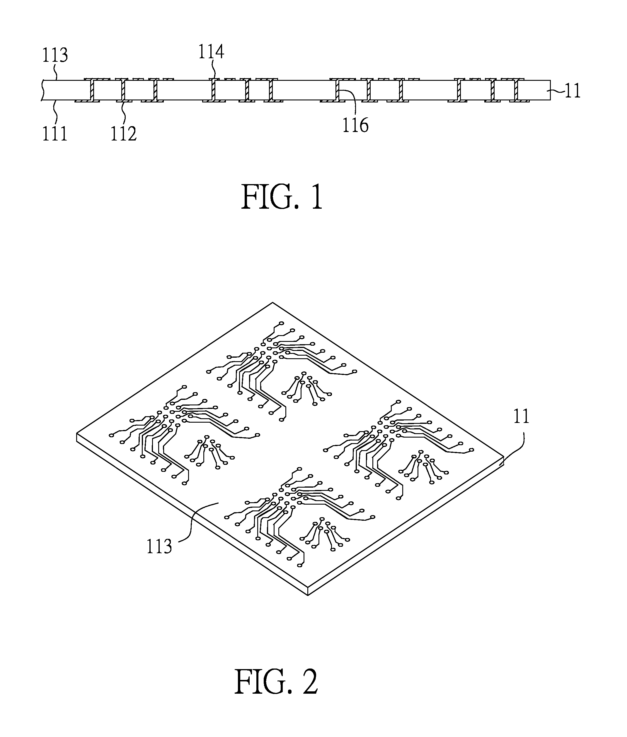
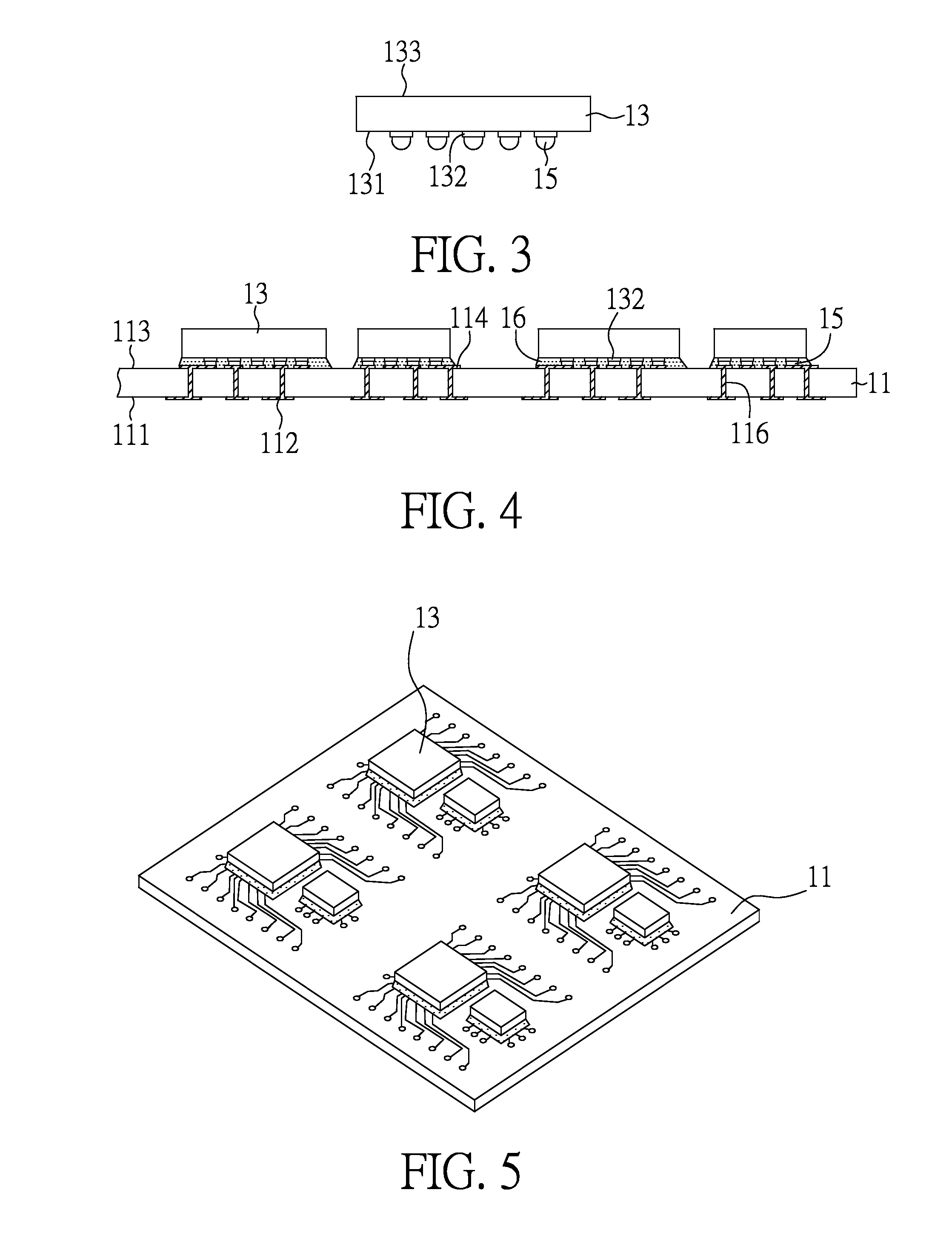
[0057]FIGS. 1-17 are schematic views showing a method of making a semiconductor package for package-on-package stacking, that includes an interposer, semiconductor devices, a base carrier, dual buildup circuitries and plated through holes in accordance with an embodiment of the present invention.

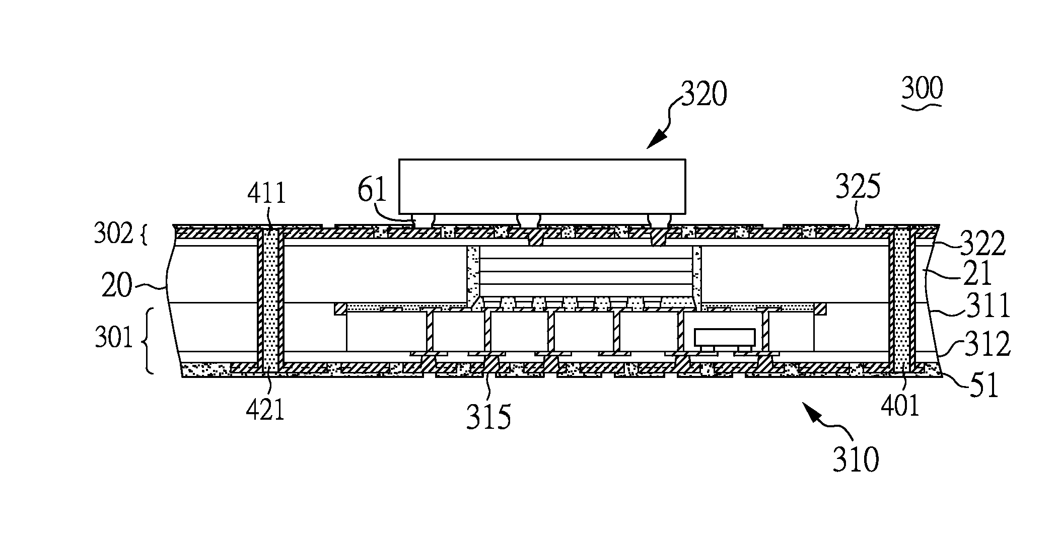
[0058]As shown in FIG. 17, the semiconductor package 110 for package-on-package stacking application includes an interposer 11′, semiconductor devices 13, a base carrier 20, a first buildup circuitry 301, a second buildup circuitry 302 and plated through holes 411. The interposer 11′ and the semiconductor devices 13 are attached to the base carrier 20 using an adhesive 191, with the semiconductor devices 13 positioned in through openings 205 of the base carrier 20. The first buildup circuitry 301 covers the interposer 11′ and the base carrier 20 from the lower side and is electrically coupled to first contact pads 112 of the interposer 11′ through first conductive vias 317, whereas the secon...

embodiment 2

[0076]FIGS. 19-27 are schematic views showing a method of making another semiconductor package with package-on-package stacking capability which has a registration mark for interposer attachment and horizontal and vertical EMI (electromagnetic interference) shields for the semiconductor devices in accordance with another embodiment of the present invention.

[0077]For purposes of brevity, any description in Embodiment 1 above is incorporated herein insofar as the same is applicable, and the same description need not be repeated.

[0078]FIGS. 19 and 20 are cross-sectional and bottom perspective views, respectively, of a base carrier 20 having through openings 205 and a registration mark 237. The through openings 205 extend through the base carrier 20 between the first surface 201 and the second surface 203 thereof, and the registration mark 237 is formed on the first surface 201. In this embodiment, the base carrier 20 includes a conductive layer 23 (typically a copper layer) on the side...

embodiment 3

[0088]FIGS. 29-38 are schematic views showing a method of making yet another semiconductor package with package-on-package stacking capability in which the base carrier is fabricated from a laminate substrate in accordance with yet another embodiment of the present invention.

[0089]For purposes of brevity, any description in the aforementioned Embodiments is incorporated herein insofar as the same is applicable, and the same description need not be repeated.

[0090]FIGS. 29 and 30 are cross-sectional views showing a process of forming a registration mark on a dielectric layer in accordance with an embodiment of the present invention.

[0091]FIG. 29 is a cross-sectional view of a laminate substrate that includes a dielectric layer 21 and a metal layer 25. The dielectric layer 21 typically is made of epoxy resin, glass-epoxy, polyimide or the like, and has a thickness of 0.5 mm in this embodiment. The metal layer 25 typically is made of copper, but copper alloys or other materials (such as...


PUM


Abstract

A method of making a semiconductor package with package-on-package stacking capability is characterized by the step of attaching a chip-on-interposer subassembly on a base carrier with the chip inserted into a through opening of the base carrier and the interposer laterally extending beyond the through opening. The interposer provides primary fan-out routing for the chip whereas dual buildup circuitries formed on both opposite sides of the base carrier provides further fan-out routing and are electrically connected to each other by plated through holes to provide the package with stacking capacity.

Description

CROSS REFERENCE TO RELATED APPLICATIONS[0001]This application claims the benefit of filing date of U.S. Provisional Application Ser. No. 61 / 911,562 filed Dec. 4, 2013. The entirety of said Provisional application is incorporated herein by reference.FIELD OF THE INVENTION[0002]The present invention relates to a semiconductor package with package-on-package stacking capability, more particularly, to a stackable semiconductor package having a semiconductor device positioned in a through opening of a base carrier and electrically connected to an interposer, and a method of making the same.DESCRIPTION OF RELATED ART[0003]The convergence of mobility, communication, and computing has created significant thermal, electrical and reliability challenges to the semiconductor packaging industry. Despite numerous package-on-package assemblies reported in the literature, many manufacturing yield-related deficiencies remain. For example, the package-on-package assemblies disclosed in U.S. Patent Pu...

Claims


Application Information

Patent Timeline
Patent Type & Authority Applications(United States)
IPC IPC(8): H01L23/00H01L21/768
CPCH01L24/81H01L24/19H01L2924/37001H01L24/17H01L24/25H01L21/76877H01L24/97H01L24/16H01L24/13H01L24/73H01L2224/13101H01L2224/16225H01L2224/32225H01L2224/73253H01L2224/73204H01L2224/81207H01L2224/81203H01L2224/81815H01L2224/92125H01L2924/171H01L2924/16195H01L2924/15173H01L2924/00012H01L2924/00014H01L2924/014H01L2924/12042H01L23/13H01L23/552H05K1/186H05K3/3436H05K3/4694H01L2924/00
Inventor LIN, CHARLES W. C.WANG, CHIA-CHUNG
Owner BRIDGE SEMICON
Why Eureka
Try Eureka