Semiconductor light-emitting element assembly

a technology of semiconductor light-emitting elements and assembly, which is applied in the direction of semiconductor devices, semiconductor/solid-state device details, electrical devices, etc., can solve the problems of too expensive ceramic materials such as aln, and the disadvantage of miniature electronic elements, so as to reduce the adverse influence and good heat dissipation of leds

Active Publication Date: 2006-04-13
EPISTAR CORP
View PDF6 Cites 86 Cited by
  • Summary
  • Abstract
  • Description
  • Claims
  • Application Information

AI Technical Summary

Benefits of technology

[0006] For overcoming the conventional problems as described in the aforementioned background, the object of the present invention is to provide a semiconductor light-emitting element assembly for achieving good heat dissipation of an LED and lessening the adverse influence resulted from the difference between the thermal expansion coefficients of different types of materials in the LED assembly.

Problems solved by technology

The mechanical method, such as screwing and buckling, needs a large space to install related mechanical devices, and thus is disadvantageous for miniature electronic elements.
However, the ceramic material such as AlN is too expensive to be acceptable to market.

Method used


Image

  • Semiconductor light-emitting element assembly
  • Semiconductor light-emitting element assembly
  • Semiconductor light-emitting element assembly

Examples


first embodiment

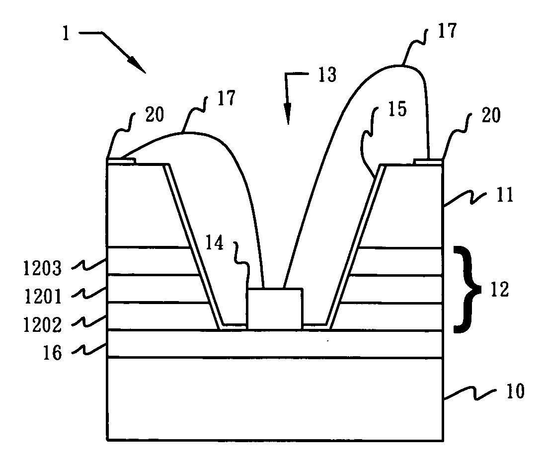
[0028]FIGS. 1A and 1B are schematic diagrams showing the structure of a semiconductor light-emitting element assembly 1 in accordance with a first embodiment of the present invention. The indications of the respective reference numbers therein are described as follows: 1 indicates a semiconductor light-emitting element assembly; 10 indicates a composite substrate; 11 indicates a circuit layout carrier; 12 indicates a connecting structure; 13 indicates a recess; 14 indicates a semiconductor light-emitting element. Further, the same reference numbers are used for the similar elements in other figures, and will not be explained again hereinafter.

[0029] A recess 13 is formed within or from a circuit layout carrier 11, and the circuit layout carrier 11 is bonded with a composite substrate 10 by a connecting structure 12. A semiconductor light-emitting element 14 is fixed within the recess 13, and conductive wires 17 are used to connect the semiconductor light-emitting element 14 to elec...

second embodiment

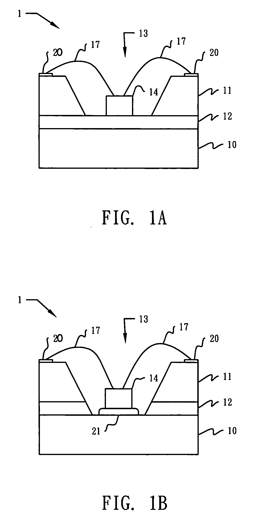
[0037]FIG. 2 is a schematic diagram showing the structure of a semiconductor light-emitting assembly 1 in accordance with a second embodiment of the present invention, wherein reference number 1201 denotes a flexible adhesive layer; 1202 and 1023 denote reaction layers; 15 denotes a reflection layer; and 16 denotes a planarizing layer.

[0038] As described in the first embodiment, the semiconductor light-emitting element 14 of the present invention is bonded with the circuit layout carrier 11 via the connecting structure 12. As shown in FIG. 2, the connecting structure 12 is composed of a flexible adhesive layer 1201, and a reaction layer 1202 and / or a reaction layer 1203 for enhancing the adhesion of connecting structure 12. The flexible adhesive layer 1201 can be formed with the material described in the first embodiment. The reaction layer 1202 is formed between the flexible adhesive layer 1201 and the circuit layout carrier 11; and / or the reaction layer 1203 is formed between the...

third embodiment

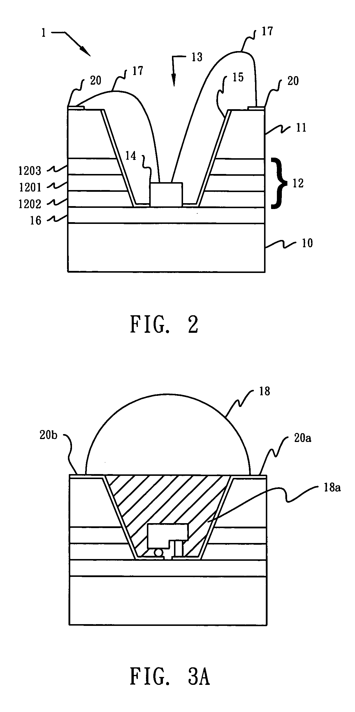
[0041]FIGS. 3A to 3H are schematic diagrams showing the structure of a semiconductor light-emitting element assembly 1 in accordance with a third embodiment of the present invention, wherein reference number 18 denotes a light pervious member; 18a denotes filling material; and 19 denotes wavelength-converting material. Such as disclosed in the aforementioned embodiments, the positive and negative electrodes of the semiconductor light-emitting element 14 are on the same side, and the conductive wires 17 are used to connect the positive and negative electrodes to the electrical contacts 20. However, the semiconductor light-emitting element 14 of the present invention is alternatively a flip-chip structure, i.e. both of the positive and negative electrodes on the same side face towards the composite substrate 10. If the semiconductor light-emitting element 14 is in the flip-chip format, the conductive wires 17 are not needed. Otherwise the electrical contact 20a has to extend to inside...


PUM


Abstract

A semiconductor light-emitting element assembly, comprising a composite substrate, a circuit layout carrier, a connecting structure, a recess, and a semiconductor light-emitting element, is disclosed. The connecting structure is used for bonding the composite substrate with the circuit layout carrier. The recess is formed by the circuit layout carrier and extends toward the composite substrate. The semiconductor light-emitting element is deposited in the recess and electrically connected to the circuit layout carrier.

Description

RELATED APPLICATIONS [0001] The present application claims the right of priority based on Taiwan Application Serial Number 093129157, filed Sep. 24, 2004; Taiwan Application Serial Number 094114630, filed May 6, 2005; Taiwan Application Serial Number 094103538, filed Feb. 4, 2005; Taiwan Application Serial Number 094121784, filed Jun. 29, 2005; and Taiwan Application Serial Number 094128644, filed Aug. 22, 2005, the disclosure of which is incorporated herein by reference in its entirety. FIELD OF THE INVENTION [0002] The present invention relates to the packaging of a semiconductor light-emitting element, and more particularly to a light-emitting element assembly comprising a composite substrate and flexible adhesive material. BACKGROUND OF THE INVENTION [0003] U.S. Pat. No. 6,501,103 discloses a light emitting diode (LED) assembly comprising a LED (1), a circuit board (2), and a heat-dissipating substrate (3), wherein the LED (1) has a die (12) bound on a heat-dissipating plate (10...

Claims


Application Information

Patent Timeline
Patent Type & Authority Applications(United States)
IPC IPC(8): H01L33/00H01L33/50H01L33/54H01L33/60H01L33/62
CPCH01L33/486H01L33/54H01L33/60H01L33/641H01L2224/48091H01L2224/73265H01L2924/00014H01L2924/01322H01L2924/00H01L2924/181H01L2924/00012
Inventor HSIEH, MIN-HSUNYIN, CHOU-CHIHWANG, CHIEN-YUANWANG, JEN-SHUITSAI, CHIA-FENHSU, CHIA-LIANG
Owner EPISTAR CORP
Why Eureka
Try Eureka