

Semiconductor resistor and method for manufacturing the same
- Summary
- Abstract
- Description
- Claims
- Application Information
AI Technical Summary
Benefits of technology
Problems solved by technology
Method used
Image

Examples
first embodiment
[0059] A GaAs MMIC in a first embodiment of the present invention is described below with reference to the diagrams.
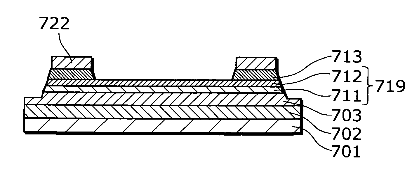
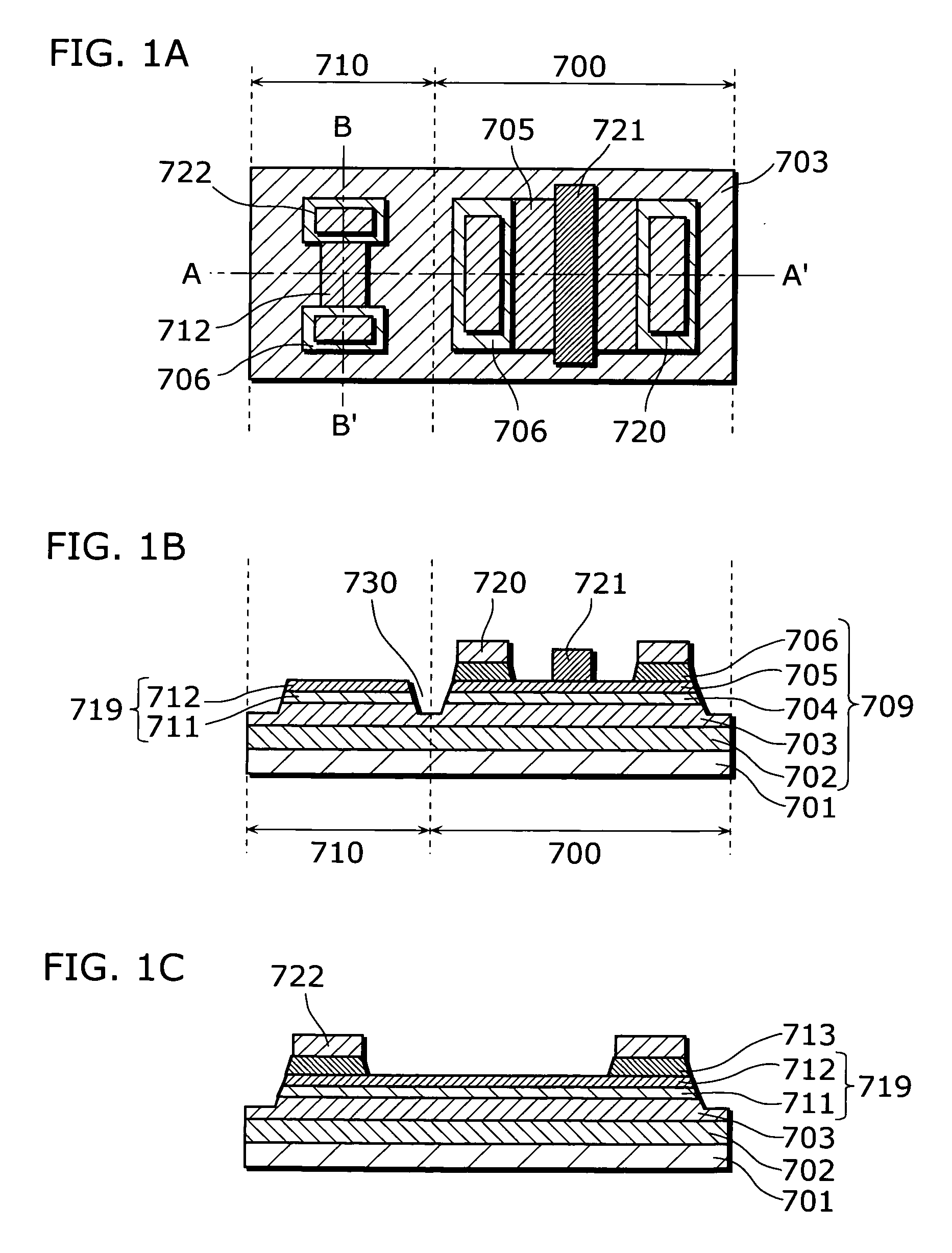
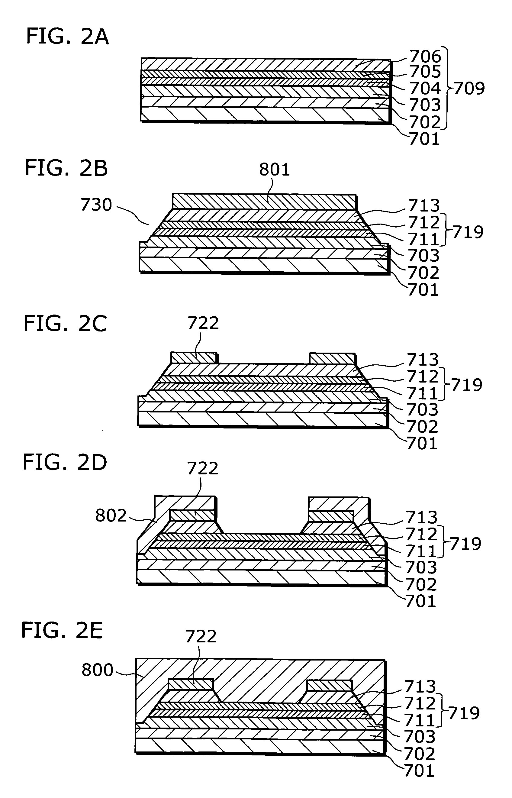
[0060]FIG. 3A is a top view of a GaAs FET as an active device and a semiconductor resistor as a passive device in the GaAs MMIC of the first embodiment, FIG. 3B is a sectional view (a section A-A′ in FIG. 3A) of the GaAs FET and the semiconductor resistor, and FIG. 3C is another sectional view (a section B-B′ in FIG. 3A) of the semiconductor resistor.
[0061] A GaAs FET 100 and a semiconductor resistor 110 are formed on the same substrate, and are electrically isolated by a device isolation region 123.
[0062] The GaAs FET 100 is composed of a substrate 101 made of semi-insulating GaAs and an epitaxial layer 109 formed by crystal growth of a semiconductor layer on the substrate 101. The epitaxial layer 109 includes the following sequentially stacked layers: a buffer layer 102 made of 1-μm-thick undoped GaAs for alleviating lattice-mismatching between the epitaxial layer...
second embodiment
[0082] A GaAs MMIC in a second embodiment of the present invention is described below with reference to the diagrams.
[0083]FIG. 6A is a top view of a GaAs FET as an active device and a semiconductor resistor as a passive device in the GaAs MMIC of the second embodiment, FIG. 6B is a sectional view (a section A-A′ in FIG. 6A) of the GaAs FET and the semiconductor resistor, and FIG. 6C is another sectional view (a section B-B′ in FIG. 6A) of the semiconductor resistor. In these diagrams, the same reference numbers are assigned to the elements common to the elements shown in FIGS. 3A to 3C, and the detailed description thereof is not repeated here.
[0084] A GaAs FET 400 and a semiconductor resistor 410 are formed on the same substrate, and are electrically isolated by the device isolation region 123.
[0085] The GaAs FET 400 is composed of the semi-insulating substrate 101 and an epitaxial layer 401 formed by crystal growth of a semiconductor layer on the substrate 101. The epitaxial l...
PUM
 Abstract
Description
Claims
Application Information